Embedded Flash memory interface RM0090
74/1749 RM0090 Rev 18
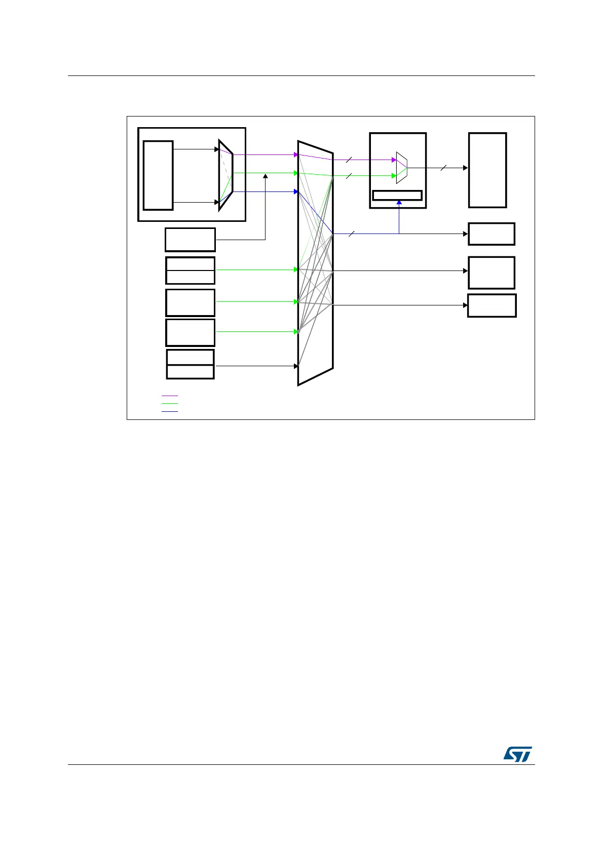
Figure 4. Flash memory interface connection inside system architecture
(STM32F42xxx and STM32F43xxx)
3.3 Embedded Flash memory in
STM32F405xx/07xx and STM32F415xx/17xx
The Flash memory has the following main features:
• Capacity up to 1 Mbyte
• 128 bits wide data read
• Byte, half-word, word and double word write
• Sector and mass erase
• Memory organization
The Flash memory is organized as follows:
– A main memory block divided into 4 sectors of 16 Kbytes, 1 sector of 64 Kbytes,
and 7 sectors of 128 Kbytes
– System memory from which the device boots in System memory boot mode
– 512 OTP (one-time programmable) bytes for user data
The OTP area contains 16 additional bytes used to lock the corresponding OTP
data block.
– Option bytes to configure read and write protection, BOR level, watchdog
software/hardware and reset when the device is in Standby or Stop mode.
• Low-power modes (for details refer to the Power control (PWR) section of the reference
manual)
Cortex
core
Ethernet
USB HS
DMA1
DMA2
D-code bus
I-Code bus
Cortex-M4 with FPU
I-Code
D-Code
S bus
AHB
periph1
Flash
memory
Flash interface
SRAM and
external
memories
AHB
periph2
FLITF registers
AHB
32-bit
instruction
bus
Access to instruction in Flash memory
Access to data and literal pool in Flash memory
FLITF register access
MS30466V3
CCM data
RAM
AHB
32-bit
data bus
AHB
32-bit
system bus
Flash
memory
bus
128 bits
DMA2D
LCD-TFT