Power controller (PWR) RM0090
116/1749 RM0090 Rev 18
5 Power controller (PWR)
This section applies to the whole STM32F4xx family, unless otherwise specified.
5.1 Power supplies
The device requires a 1.8 to 3.6 V operating voltage supply (V
DD
). An embedded linear
voltage regulator is used to supply the internal 1.2 V digital power.
The real-time clock (RTC), the RTC backup registers, and the backup SRAM (BKP SRAM)
can be powered from the V
BAT
voltage when the main V
DD
supply is powered off.
Note: Depending on the operating power supply range, some peripheral may be used with limited
functionality and performance. For more details refer to section “General operating
conditions” in STM32F4xx datasheets.
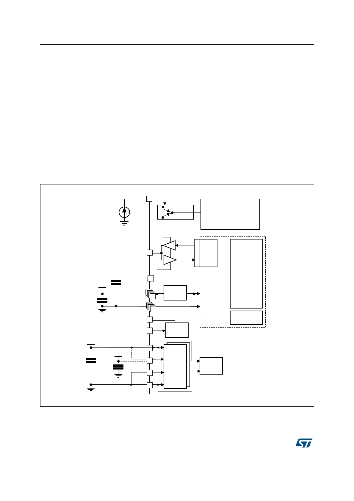
Figure 9. Power supply overview for STM32F405xx/07xx and STM32F415xx/17xx
1. V
DDA
and V
SSA
must be connected to V
DD
and V
SS
, respectively.
MS19911V2
Backup circuitry
(OSC32K,RTC,
Wakeup logic
Backup registers,
backup RAM)
Kernel logic
(CPU, digital
& RAM)
Analog:
RCs,
PLL,..
Power
switch
VBAT
GPIOs
OUT
IN
15 × 100 nF
+ 1 × 4.7 μF
VBAT =
1.65 to 3.6V
Voltage
regulator
VDDA
ADC
Level shifter
IO
Logic
VDD
100 nF
+ 1 μF
Flash memory
VCAP_1
VCAP_2
2 × 2.2 μF
BYPASS_REG
PDR_ON
Reset
controller
VDD
1/2/...14/15
VSS
1/2/...14/15
VDD
VREF+
VREF-
VSSA
VREF
100 nF
+ 1 μF