Analog-to-digital converter (ADC) RM0090
432/1749 RM0090 Rev 18
Refer to Section 2.3: Memory map for the register boundary addresses.
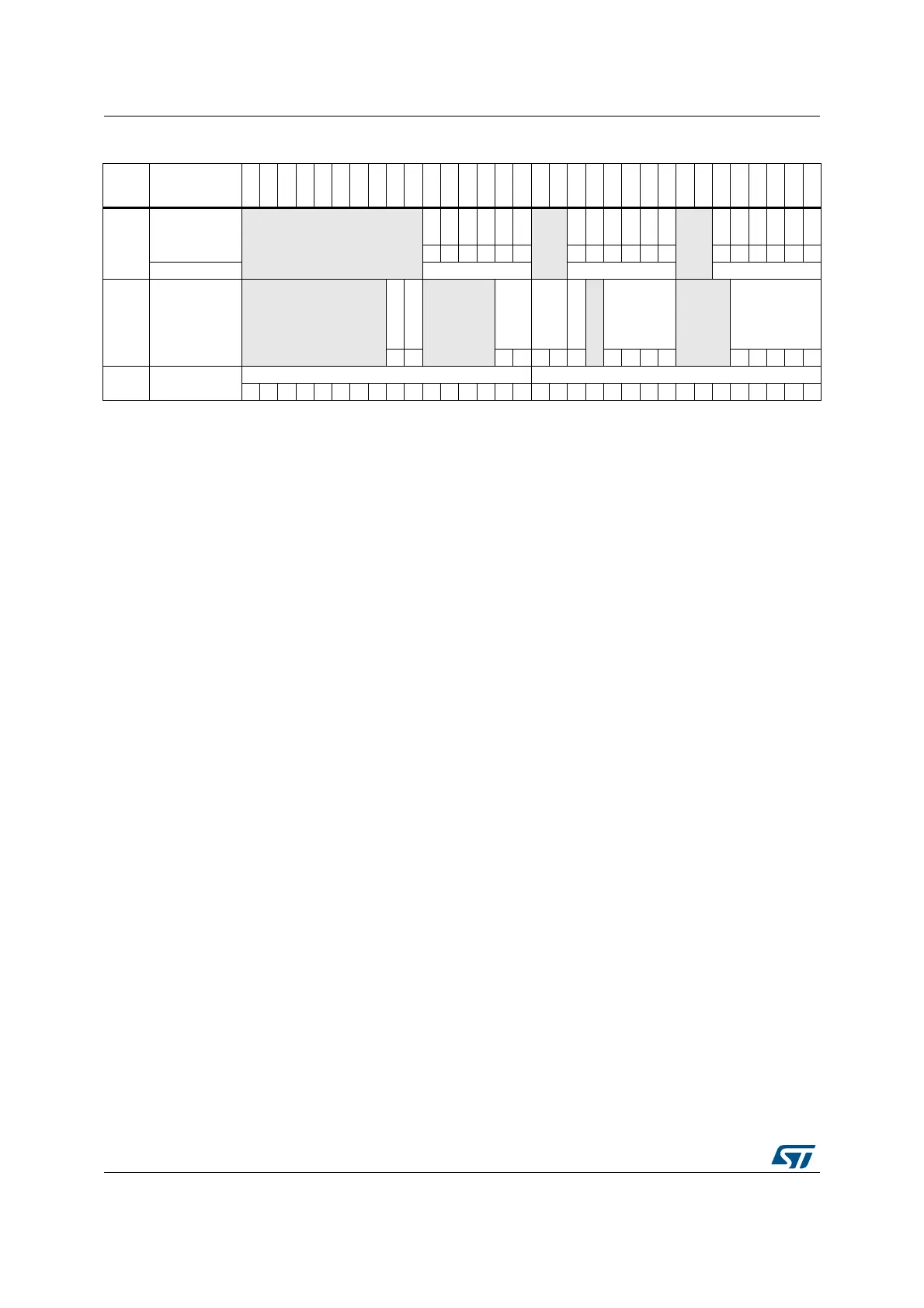
Table 73. ADC register map and reset values (common ADC registers)
Offset Register
31
30
29
28
27
26
25
24
23
22
21
20
19
18
17
16
15
14
13
12
11
10
9
8
7
6
5
4
3
2
1
0
0x00
ADC_CSR
Reserved
OVR
STRT
JSTRT
JEOC
EOC
AWD
Reserved
OVR
STRT
JSTRT
JEOC
EOC
AWD
Reserved
OVR
STRT
JSTRT
JEOC
EOC
AWD
Reset value 000000 000000 000000
ADC3 ADC2 ADC1
0x04
ADC_CCR
Reserved
TSVREFE
VBATE
Reserved
ADCPRE[1:0]
DMA[1:0]
DDS
Reserved
DELAY [3:0]
Reserved
MULTI [4:0]
Reset value 00 00000 0000 00000
0x08
ADC_CDR Regular DATA2[15:0] Regular DATA1[15:0]
Reset value 00000000000000000000000000000000