General-purpose timers (TIM2 to TIM5) RM0090
606/1749 RM0090 Rev 18
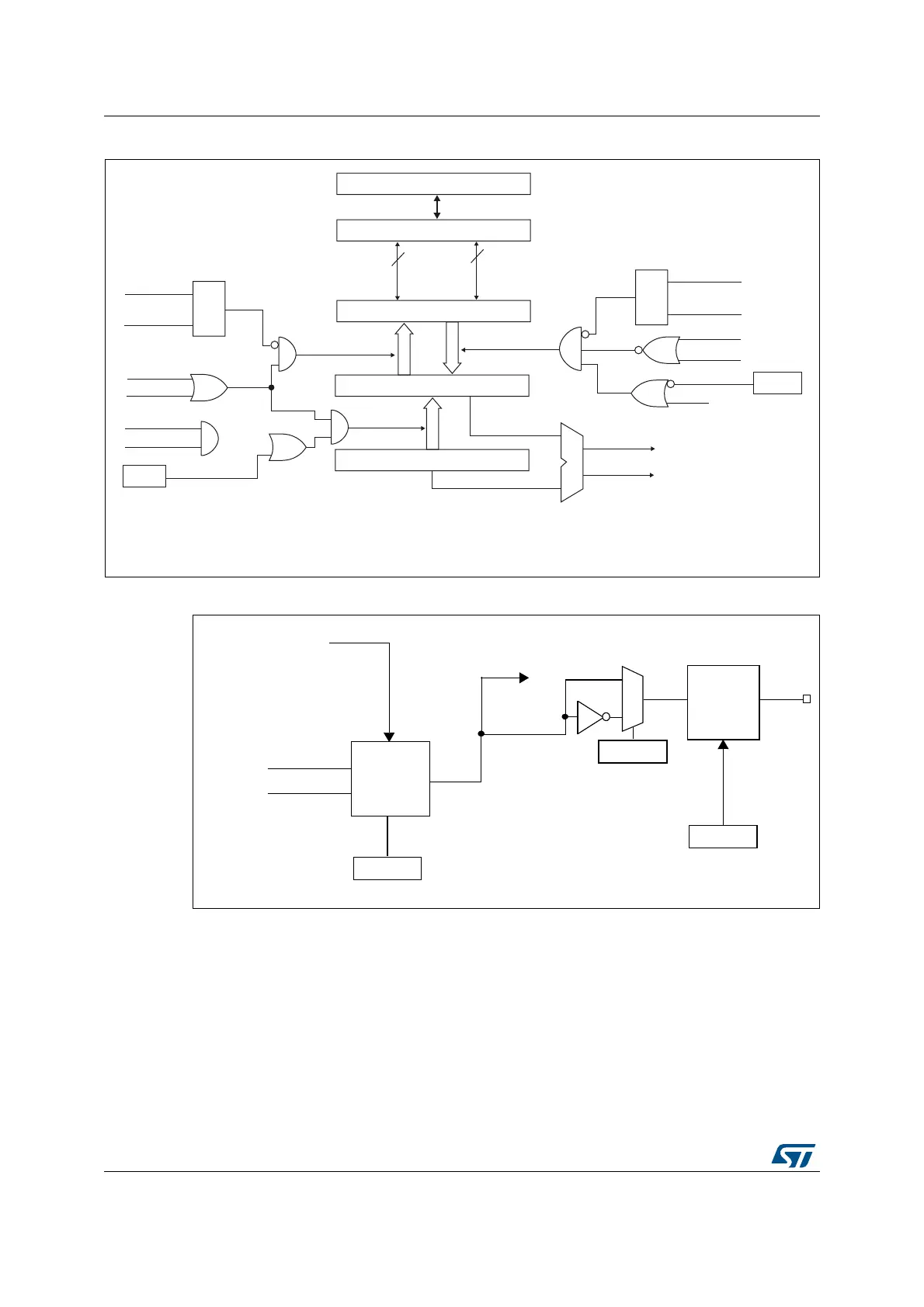
Figure 160. Capture/compare channel 1 main circuit
Figure 161. Output stage of capture/compare channel (channel 1)
The capture/compare block is made of one preload register and one shadow register. Write
and read always access the preload register.
In capture mode, captures are actually done in the shadow register, which is copied into the
preload register.
In compare mode, the content of the preload register is copied into the shadow register
which is compared to the counter.
CC1E
Capture/compare shadow register
Comparator
Capture/compare preload register
Counter
IC1PS
CC1S[0]
CC1S[1]
Capture
Input
mode
S
R
Read CCR1H
Read CCR1L
read_in_progress
capture_transfer
CC1S[0]
CC1S[1]
S
R
write CCR1H
write CCR1L
write_in_progress
Output
mode
UEV
OC1PE
(from time
base unit)
compare_transfer
APB Bus
8
8
high
low
(if 16-bit)
MCU-peripheral interface
TIMx_CCMR1
OC1PE
CNT>CCR1
CNT=CCR1
TIMx_EGR
CC1G
MS33144V1
Output mode
TIMx_CNT > TIMx_CCR1
controller
TIMx_CCMR1
OC1M[2:0]
oc1ref
0
1
TIMx_CCER
Output
Enable
Circuit
OC1
TIMx_CCER
To the master mode
controller
ETRF
ai17187b
CC1P
CC1E
TIMx_CNT = TIMx_CCR1