Flexible memory controller (FMC) RM0090
1636/1749 RM0090 Rev 18
The FMC supports both NOR Flash wait state configurations, for each Chip Select, thanks
to the WAITCFG bit in the FMC_BCRx registers (x = 0..3).
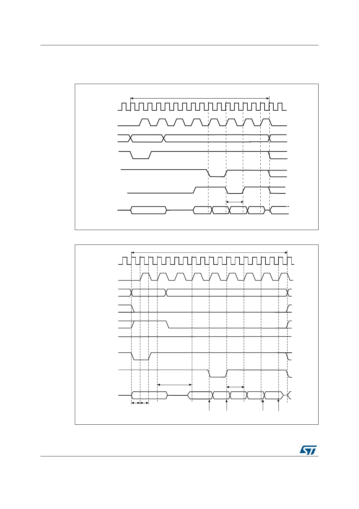
Figure 473. Wait configuration waveforms
Figure 474. Synchronous multiplexed read mode waveforms - NOR, PSRAM (CRAM)
1. Byte lane outputs BL are not shown; for NOR access, they are held high, and, for PSRAM (CRAM) access,
addr[15:0] data data
addr[25:16]
Memory transaction = burst of 4 half words
HCLK
CLK
A[25:16]
NADV
NWAIT
(WAITCFG = 1)
A/D[15:0]
inserted wait state
data
NWAIT
(WAITCFG = 0)
ai15798c
Addr[15:0] data data
addr[25:16]
Memory transaction = burst of 4 half words
HCLK
CLK
A[25:16]
NEx
NOE
NWE
High
NADV
NWAIT
(WAITCFG=
0)
A/D[15:0]
1 clock
cycle
1 clock
cycle
(DATLAT + 2)
inserted wait state
Data strobes
ai17723f
CLK cycles
data data
Data strobes