Serial peripheral interface (SPI) RM0090
882/1749 RM0090 Rev 18
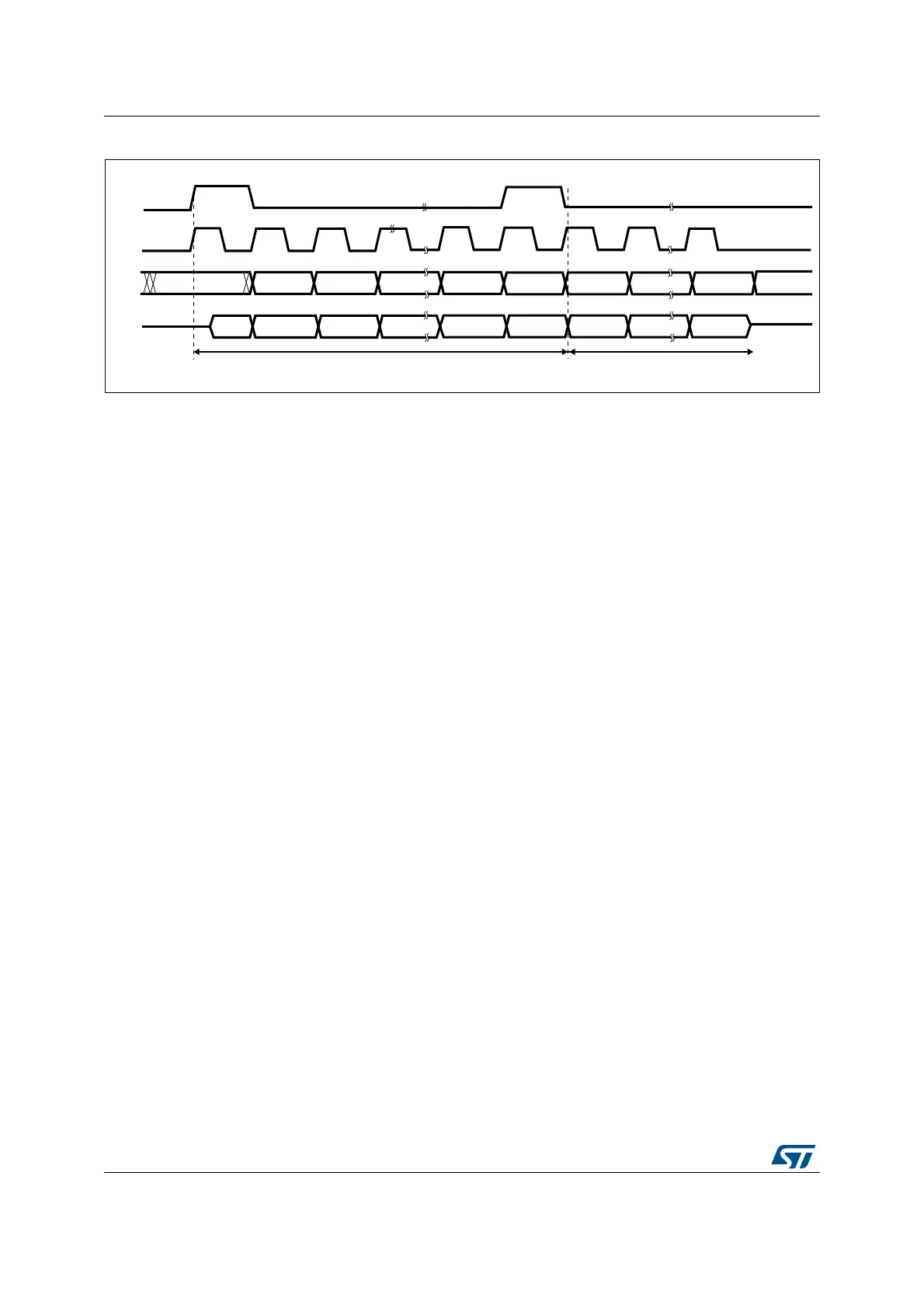
Figure 250. TI mode - Slave mode, continuous transfer
28.3.3 Configuring the SPI in master mode
In the master configuration, the serial clock is generated on the SCK pin.
Procedure
1. Select the BR[2:0] bits to define the serial clock baud rate (see SPI_CR1 register).
2. Select the CPOL and CPHA bits to define one of the four relationships between the
data transfer and the serial clock (see Figure 248). This step is not required when the
TI mode is selected.
3. Set the DFF bit to define 8- or 16-bit data frame format
4. Configure the LSBFIRST bit in the SPI_CR1 register to define the frame format. This
step is not required when the TI mode is selected.
5. If the NSS pin is required in input mode, in hardware mode, connect the NSS pin to a
high-level signal during the complete byte transmit sequence. In NSS software mode,
set the SSM and SSI bits in the SPI_CR1 register. If the NSS pin is required in output
mode, the SSOE bit only should be set. This step is not required when the TI mode is
selected.
6. Set the FRF bit in SPI_CR2 to select the TI protocol for serial communications.
7. The MSTR and SPE bits must be set (they remain set only if the NSS pin is connected
to a high-level signal).
In this configuration the MOSI pin is a data output and the MISO pin is a data input.
Transmit sequence
The transmit sequence begins when a byte is written in the Tx Buffer.
The data byte is parallel-loaded into the shift register (from the internal bus) during the first
bit transmission and then shifted out serially to the MOSI pin MSB first or LSB first
depending on the LSBFIRST bit in the SPI_CR1 register. The TXE flag is set on the transfer
of data from the Tx Buffer to the shift register and an interrupt is generated if the TXEIE bit in
the SPI_CR2 register is set.
ai18435
MSBIN
MOSI
input
NSS
input
SCK
input
trigger sampling trigger sampling trigger sampling
DONTCARE LSBIN
DONTCARE
MISO
output
1 or 0 MSBOUT
LSBOUT
MSBIN LSBIN
MSBOUT
LSBOUT
FRAME 1 FRAME 2