RM0090 Rev 18 539/1749
RM0090 Advanced-control timers (TIM1 and TIM8)
588
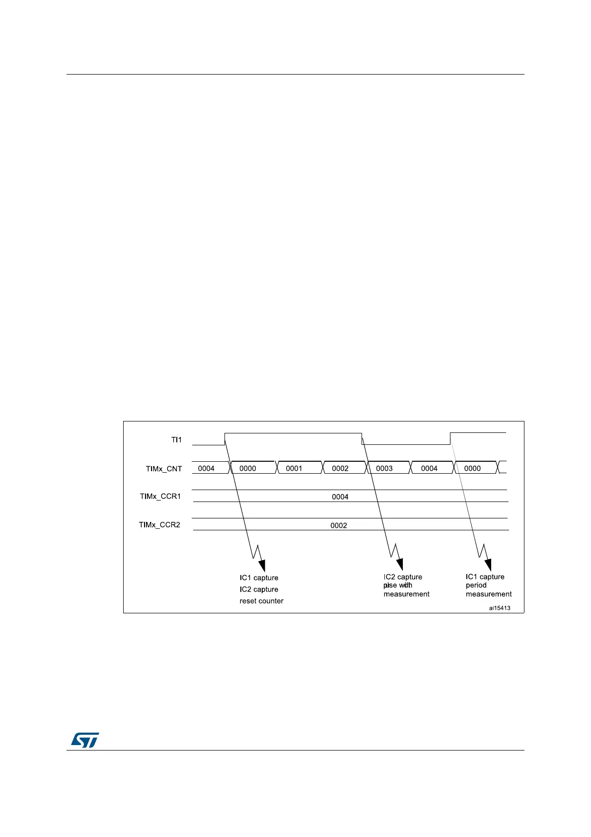
17.3.7 PWM input mode
This mode is a particular case of input capture mode. The procedure is the same except:
• Two ICx signals are mapped on the same TIx input.
• These 2 ICx signals are active on edges with opposite polarity.
• One of the two TIxFP signals is selected as trigger input and the slave mode controller
is configured in reset mode.
For example, user can measure the period (in TIMx_CCR1 register) and the duty cycle (in
TIMx_CCR2 register) of the PWM applied on TI1 using the following procedure (depending
on CK_INT frequency and prescaler value):
• Select the active input for TIMx_CCR1: write the CC1S bits to 01 in the TIMx_CCMR1
register (TI1 selected).
• Select the active polarity for TI1FP1 (used both for capture in TIMx_CCR1 and counter
clear): write the CC1P and CC1NP bits to ‘0’ (active on rising edge).
• Select the active input for TIMx_CCR2: write the CC2S bits to 10 in the TIMx_CCMR1
register (TI1 selected).
• Select the active polarity for TI1FP2 (used for capture in TIMx_CCR2): write the CC2P
and CC2NP bits to ‘1’ (active on falling edge).
• Select the valid trigger input: write the TS bits to 101 in the TIMx_SMCR register
(TI1FP1 selected).
• Configure the slave mode controller in reset mode: write the SMS bits to 100 in the
TIMx_SMCR register.
• Enable the captures: write the CC1E and CC2E bits to ‘1’ in the TIMx_CCER register.
Figure 116. PWM input mode timing
17.3.8 Forced output mode
In output mode (CCxS bits = 00 in the TIMx_CCMRx register), each output compare signal
(OCxREF and then OCx/OCxN) can be forced to active or inactive level directly by software,
independently of any comparison between the output compare register and the counter.
To force an output compare signal (OCXREF/OCx) to its active level, the user just needs to
write 101 in the OCxM bits in the corresponding TIMx_CCMRx register. Thus OCXREF is