Flexible memory controller (FMC) RM0090
1634/1749 RM0090 Rev 18
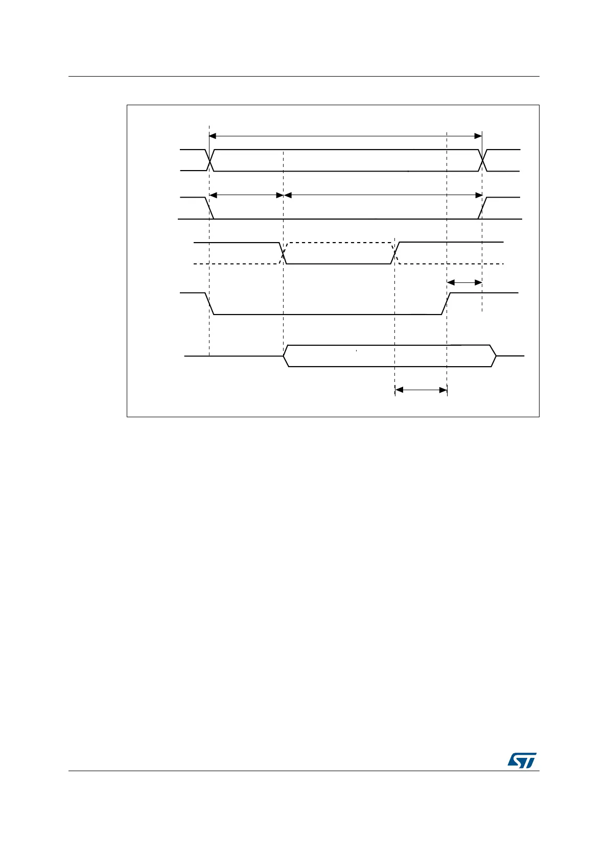
Figure 472. Asynchronous wait during a write access waveforms
1. NWAIT polarity depends on WAITPOL bit setting in FMC_BCRx register.
37.5.5 Synchronous transactions
The memory clock, FMC_CLK, is a submultiple of HCLK. It depends on the value of
CLKDIV and the MWID/ AHB data size, following the formula given below:
If MWID is 16 or 8 bits, the FMC_CLK divider ratio is always defined by the programmed
CLKDIV value.
If MWID is 32 bits, the FMC_CLK divider ratio depends also on AHB data size.
Example:
• If CLKDIV=1, MWID=32 bits, AHB data size=8 bits, FMC_CLK=HCLK/4.
• If CLKDIV=1, MWID=16 bits, AHB data size=8 bits, FMC_CLK=HCLK/2.
NOR Flash memories specify a minimum time from NADV assertion to CLK high. To meet
this constraint, the FMC does not issue the clock to the memory during the first internal
clock cycle of the synchronous access (before NADV assertion). This guarantees that the
rising edge of the memory clock occurs in the middle of the NADV low pulse.
Data latency versus NOR memory latency
The data latency is the number of cycles to wait before sampling the data. The DATLAT
value must be consistent with the latency value specified in the NOR Flash configuration
A[25:0]
NWE
Memory transaction
D[15:0]
NEx
data driven by FSMC
MS30464V2
3HCLK
address phase
data setup phase
1HCLK
NWAIT
don’t care don’t care
FMC_CLK divider ratio max CLKDIV 1+ MWID AHB data size()(, )=