RM0090 Rev 18 1587/1749
RM0090 Flexible static memory controller (FSMC)
1601
36.6.2 NAND Flash / PC Card supported memories and transactions
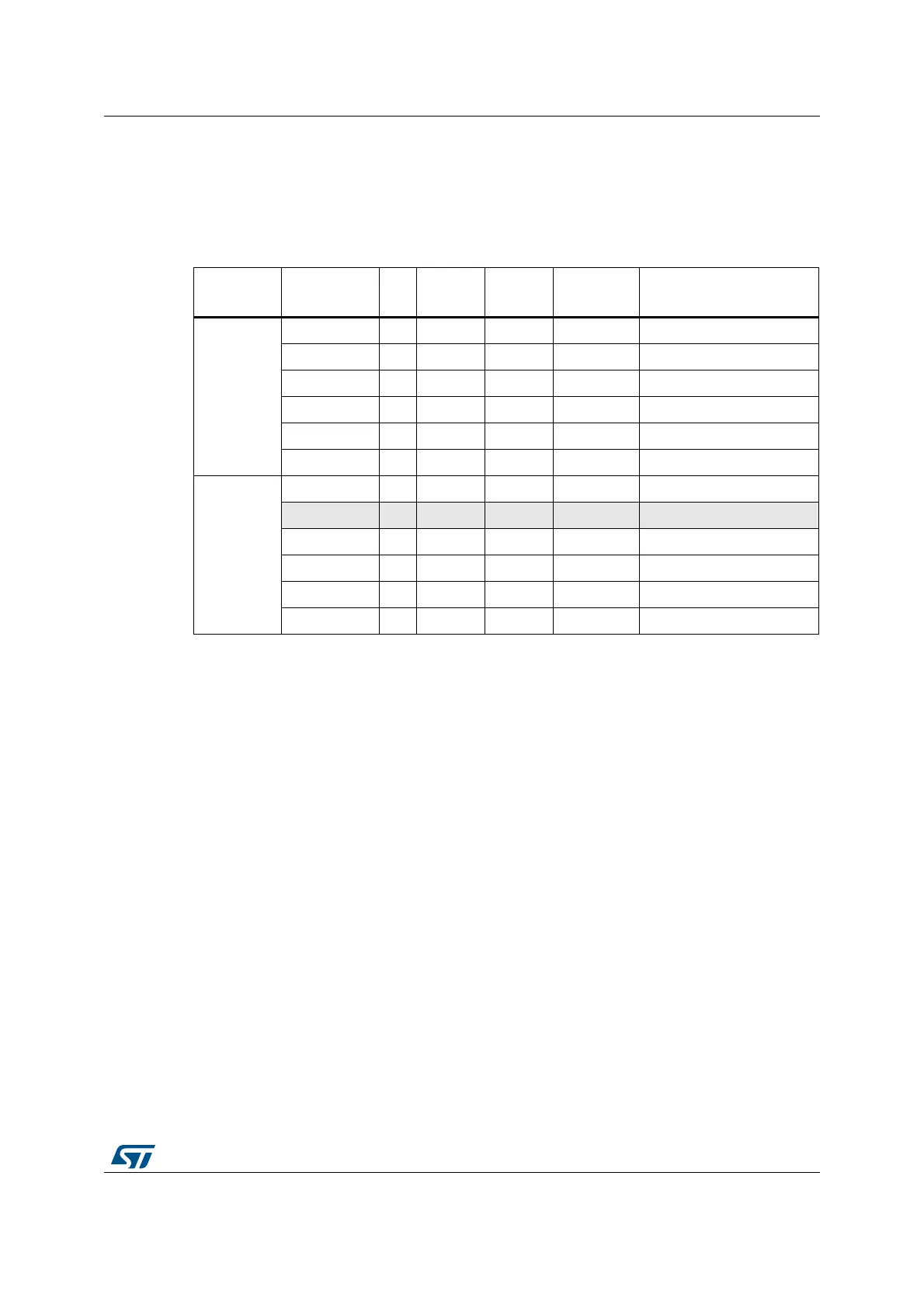
Table 250 below shows the supported devices, access modes and transactions.
Transactions not allowed (or not supported) by the NAND Flash / PC Card controller appear
in gray.
36.6.3 Timing diagrams for NAND and PC Card
Each PC Card/CompactFlash and NAND Flash memory bank is managed through a set of
registers:
• Control register: FSMC_PCRx
• Interrupt status register: FSMC_SRx
• ECC register: FSMC_ECCRx
• Timing register for Common memory space: FSMC_PMEMx
• Timing register for Attribute memory space: FSMC_PATTx
• Timing register for I/O space: FSMC_PIOx
Each timing configuration register contains three parameters used to define number of
HCLK cycles for the three phases of any PC Card/CompactFlash or NAND Flash access,
plus one parameter that defines the timing for starting driving the databus in the case of a
write. Figure 454 shows the timing parameter definitions for common memory accesses,
knowing that Attribute and I/O (only for PC Card) memory space access timings are similar.
Table 250. Supported memories and transactions
Device Mode R/W
AHB
data size
Memory
data size
Allowed/
not allowed
Comments
NAND 8-bit
Asynchronous R 8 8 Y
Asynchronous W 8 8 Y
Asynchronous R 16 8 Y Split into 2 FSMC accesses
Asynchronous W 16 8 Y Split into 2 FSMC accesses
Asynchronous R 32 8 Y Split into 4 FSMC accesses
Asynchronous W 32 8 Y Split into 4 FSMC accesses
NAND 16-bit
Asynchronous R 8 16 Y
Asynchronous W 8 16 N
Asynchronous R 16 16 Y
Asynchronous W 16 16 Y
Asynchronous R 32 16 Y Split into 2 FSMC accesses
Asynchronous W 32 16 Y Split into 2 FSMC accesses