Embedded Flash memory interface RM0090
110/1749 RM0090 Rev 18
3.9.11 Flash option control register (FLASH_OPTCR1)
for STM32F42xxx and STM32F43xxx
This register is available only on STM32F42xxx and STM32F43xxx.
The FLASH_OPTCR1 register is used to modify the user option bytes for bank 2.
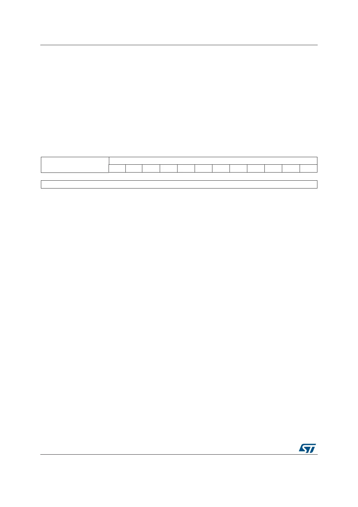
Address offset: 0x18
Reset value: 0x0FFF 0000. The option bits are loaded with values from Flash memory at
reset release.
Access: no wait state when no Flash memory operation is ongoing, word, half-word and
byte access.
31 30 29 28 27 26 25 24 23 22 21 20 19 18 17 16
Reserved
nWRP[11:0]
rw rw rw rw rw rw rw rw rw rw rw rw
15 14 13 12 11 10 9 8 7 6 5 4 3 2 1 0
Reserved
Bits 31:28 Reserved, must be kept cleared.
Bits 27:16 nWRP[11:0]: Not write protect
These bits contain the value of the write-protection and read-protection (PCROP) option bytes
for sectors 0 to 11 after reset. They can be written to program a new write-protect or PCROP
value into Flash memory.
If SPRMOD is reset (default value):
0: Write protection active on sector i.
1: Write protection not active on sector i.
If SPRMOD is set:
0: PCROP protection not active on sector i.
1: PCROP protection active on sector i.
Bits 15:0 Reserved, must be kept cleared.