RM0090 Rev 18 269/1749
RM0090 General-purpose I/Os (GPIO)
288
8.3.1 General-purpose I/O (GPIO)
During and just after reset, the alternate functions are not active and the I/O ports are
configured in input floating mode.
The debug pins are in AF pull-up/pull-down after reset:
• PA15: JTDI in pull-up
• PA14: JTCK/SWCLK in pull-down
• PA13: JTMS/SWDAT in pull-up
• PB4: NJTRST in pull-up
• PB3: JTDO in floating state
When the pin is configured as output, the value written to the output data register
(GPIOx_ODR) is output on the I/O pin. It is possible to use the output driver in push-pull
mode or open-drain mode (only the N-MOS is activated when 0 is output).
The input data register (GPIOx_IDR) captures the data present on the I/O pin at every AHB1
clock cycle.
All GPIO pins have weak internal pull-up and pull-down resistors, which can be activated or
not depending on the value in the GPIOx_PUPDR register.
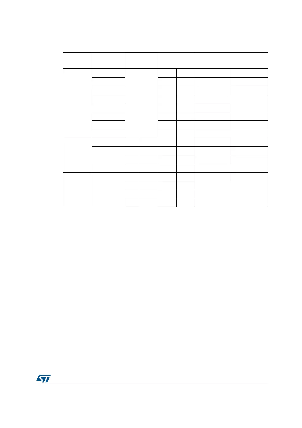
10
0
SPEED
[B:A]
0 0 AF PP
001AFPP + PU
010AFPP + PD
0 1 1 Reserved
100AFOD
101AFOD + PU
110AFOD + PD
1 1 1 Reserved
00
x x x 0 0 Input Floating
x x x 0 1 Input PU
x x x 1 0 Input PD
x x x 1 1 Reserved (input floating)
11
x x x 0 0 Input/output Analog
xxx01
Reservedxxx10
xxx11
1. GP = general-purpose, PP = push-pull, PU = pull-up, PD = pull-down, OD = open-drain, AF = alternate
function.
Table 35. Port bit configuration table
(1)
(continued)
MODER(i)
[1:0]
OTYPER(i)
OSPEEDR(i)
[B:A]
PUPDR(i)
[1:0]
I/O configuration