RM0090 Rev 18 1663/1749
RM0090 Flexible memory controller (FMC)
1682
37.7 SDRAM controller
37.7.1 SDRAM controller main features
The main features of the SDRAM controller are the following:
• Two SDRAM banks with independent configuration
• 8-bit, 16-bit, 32-bit data bus width
• 13-bits Address Row, 11-bits Address Column, 4 internal banks: 4x16Mx32bit
(256 MB), 4x16Mx16bit (128 MB), 4x16Mx8bit (64 MB)
• Word, half-word, byte access
• SDRAM clock can be HCLK/2 or HCLK/3
• Automatic row and bank boundary management
• Multibank ping-pong access
• Programmable timing parameters
• Automatic Refresh operation with programmable Refresh rate
• Self-refresh mode
• Power-down mode
• SDRAM power-up initialization by software
• CAS latency of 1,2,3
• Cacheable Read FIFO with depth of 6 lines x32-bit (6 x14-bit address tag)
37.7.2 SDRAM External memory interface signals
At startup, the SDRAM I/O pins used to interface the FMC SDRAM controller with the
external SDRAM devices must configured by the user application. The SDRAM controller
I/O pins which are not used by the application, can be used for other purposes.
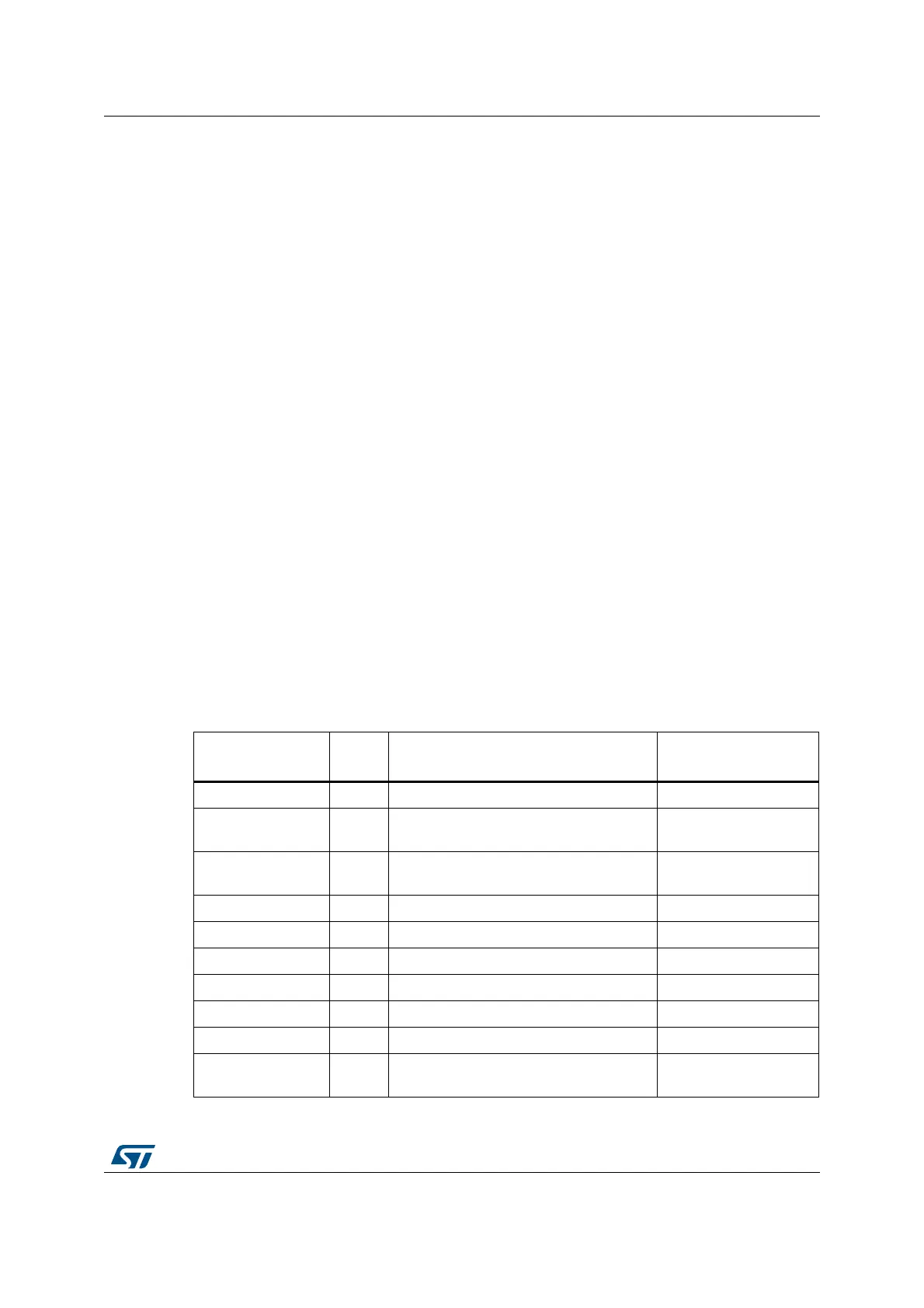
Table 296. SDRAM signals
SDRAM signal
I/O
type
Description Alternate function
SDCLK O SDRAM clock
SDCKE[1:0] O
SDCKE0: SDRAM Bank 1 Clock Enable
SDCKE1: SDRAM Bank 2 Clock Enable
SDNE[1:0] O
SDNE0: SDRAM Bank 1 Chip Enable
SDNE1: SDRAM Bank 2 Chip Enable
A[12:0] O Address FMC_A[12:0]
D[31:0] I/O Bidirectional data bus FMC_D[31:0]
BA[1:0] O Bank Address FMC_A[15:14]
NRAS O Row Address Strobe
NCAS O Column Address Strobe
SDNWE O Write Enable
NBL[3:0] O
Output Byte Mask for write accesses
(memory signal name: DQM[3:0])
FMC_NBL[3:0]