RM0090 Rev 18 537/1749
RM0090 Advanced-control timers (TIM1 and TIM8)
588
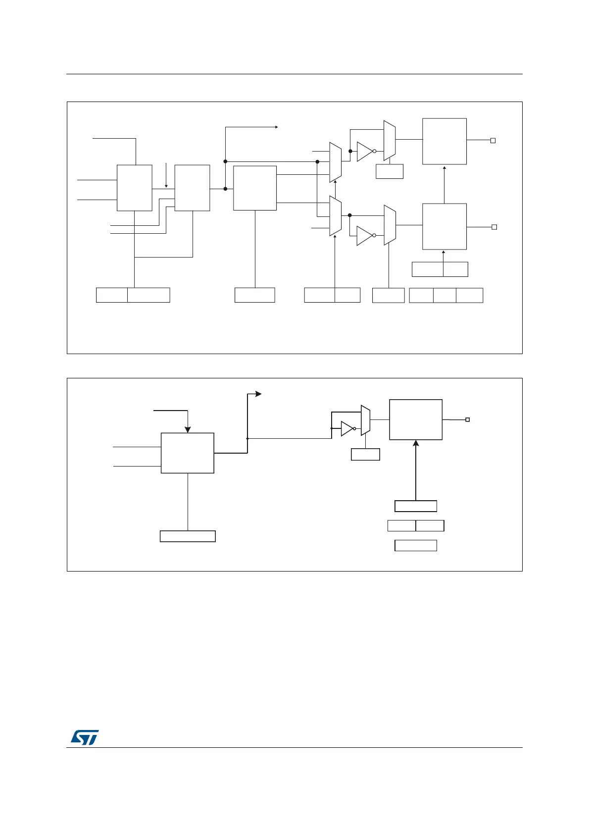
Figure 114. Output stage of capture/compare channel (channel 1 to 3)
Figure 115. Output stage of capture/compare channel (channel 4)
The capture/compare block is made of one preload register and one shadow register. Write
and read always access the preload register.
In capture mode, captures are actually done in the shadow register, which is copied into the
preload register.
In compare mode, the content of the preload register is copied into the shadow register
which is compared to the counter.
MS35909V1
Output
mode
controller
CNT>CCR1
CNT=CCR1
TIM1_CCMR1
OC1M[3:0]
OC1REF
OC1CE
Dead-time
generator
OC1_DT
OC1N_DT
DTG[7:0]
TIM1_BDTR
‘0’
‘0’
CC1E
TIM1_CCER
CC1NE
0
1
CC1P
TIM1_CCER
0
1
CC1NP
TIM1_CCER
OC1
Output
enable
circuit
OC1N
CC1E
TIM1_CCER
CC1NE
OSSI
TIM1_BDTR
MOE OSSR
0x
10
11
11
01
x0
Output
selector
OCxREF
OC1REFC
To the master mode
controller
Output
enable
circuit
OC5REF
(1)
ETRF
MS37370V1
Output
mode
controller
TIM1_CCMR2
OC1M[3:0]
OC4REF
0
1
CC4P
TIM1_CCER
OC4
To the master
mode controller
Output
enable
circuit
ETR
CNT>CCR4
CNT>CCR4
TIM1_CCER
TIM1_BDTR
TIM1_CR2
OSSIMOE
CC4E
OIS4