USB on-the-go high-speed (OTG_HS) RM0090
1384/1749 RM0090 Rev 18
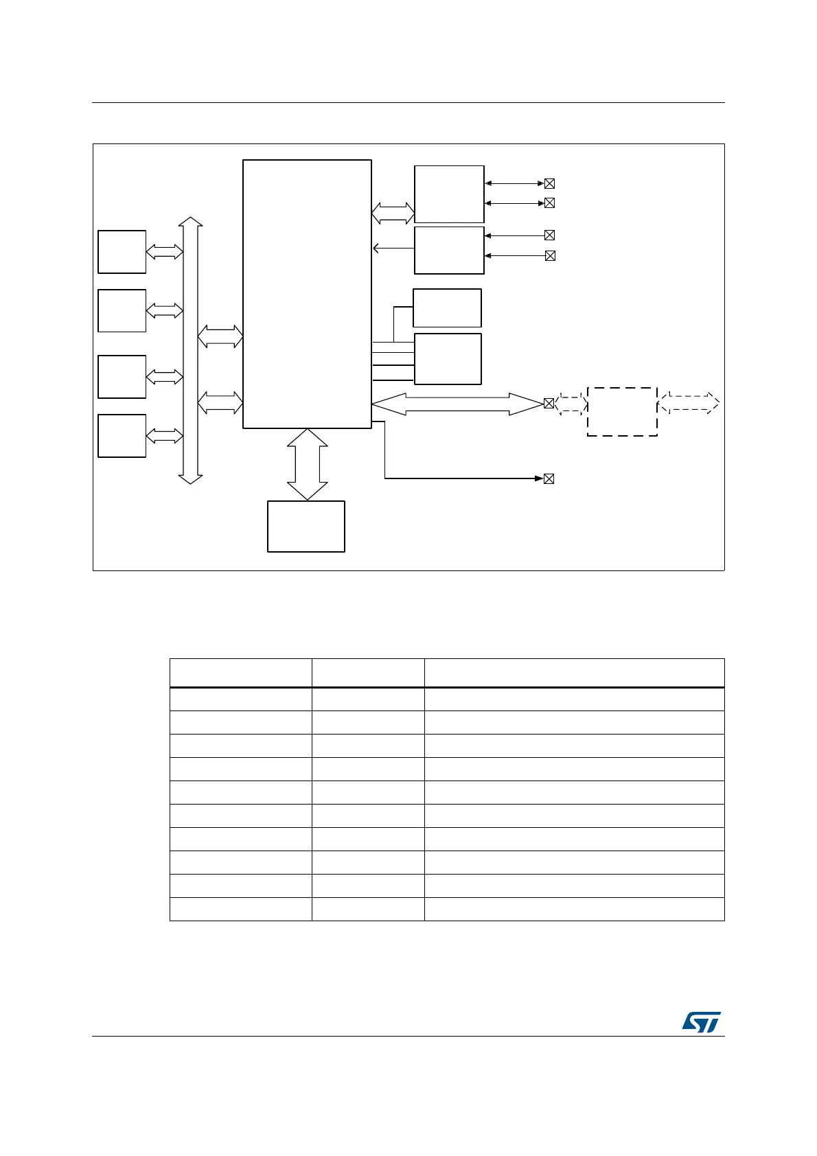
Figure 410. USB OTG interface block diagram
1. The USB DMA cannot directly address the internal Flash memory.
35.3.1 OTG pins
35.3.2 High-speed OTG PHY
The USB OTG HS core embeds an ULPI interface to connect an external HS phy.
MSv43325V1
Data FIFO
Single-port RAM
(SPRAM)
AHB
master
interface
AHB
slave
interface
CPU
Memory
Peripheral 1
Peripheral 2
Data FIFO
RAM interface
AHB (application bus)
OTG_HS
(USB OTG HS core)
OTG_HS_DP
OTG_HS_DM
OTG_HS_ID
OTG_HS_VBUS
OTG FS PHY
transceiver
OTG_HS_SOF
ULPI interface (12 pins)
ULPI PHY
(external
component)
USB2.0 (D+/D-)
ULPI_CK;
ULPI_DIR;
ULPI_STP;
ULPI_NXT;
ULPI_D0-7
NVIC
Interrupt: EP1 out
Interrupt: EP1 in
Interrupt: global
Interrupt: async wakeup
OTG detections
EXTIEXTI
serial
Table 206. OTG_HS input/output pins
Signal name Signal type Description
OTG_HS_DP Digital input/output USB OTG D+ line
OTG_HS_DM Digital input/output USB OTG D- line
OTG_HS_ID Digital input USB OTG ID
OTG_HS_VBUS Analog input USB OTG VBUS
OTG_HS_SOF Digital output USB OTG Start Of Frame (visibility)
OTG_HS_ULPI_CK Digital input USB OTG ULPI clock
OTG_HS_ULPI_DIR Digital input USB OTG ULPI data bus direction control
OTG_HS_ULPI_STP Digital output USB OTG ULPI data stream stop
OTG_HS_ULPI_NXT Digital input USB OTG ULPI next data stream request
OTG_HS_ULPI_D[0..7] Digital input/output USB OTG ULPI 8-bit bi-directional data bus