Embedded Flash memory interface RM0090
106/1749 RM0090 Rev 18
3.9.9 Flash option control register (FLASH_OPTCR) for
STM32F405xx/07xx and STM32F415xx/17xx
The FLASH_OPTCR register is used to modify the user option bytes.
Address offset: 0x14
Reset value: 0x0FFF AAED. The option bits are loaded with values from Flash memory at
reset release.
Access: no wait state when no Flash memory operation is ongoing, word, half-word and
byte access.
Bits 7:3 SNB[3:0]: Sector number
These bits select the sector to erase.
0000: sector 0
0001: sector 1
...
01011: sector 11
01100: not allowed
01101: not allowed
01110: not allowed
01111: not allowed
10000: section 12
10001: section 13
...
11011 sector 23
11100: not allowed
11101: not allowed
11110: not allowed
11111: not allowed
Bit 2 MER: Mass Erase of bank 1 sectors
Erase activated of bank 1 sectors.
Bit 1 SER: Sector Erase
Sector Erase activated.
Bit 0 PG: Programming
Flash programming activated.
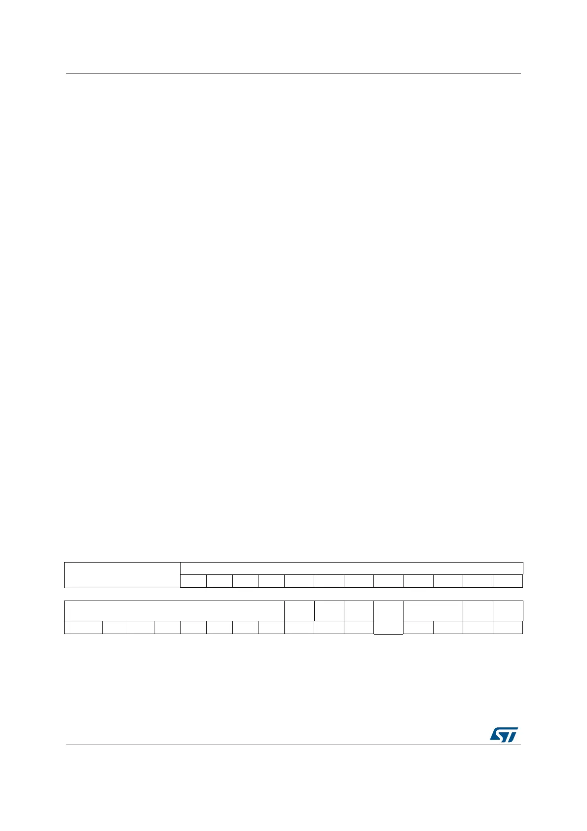
31 30 29 28 27 26 25 24 23 22 21 20 19 18 17 16
Reserved
nWRP[11:0]
rw rw rw rw rw rw rw rw rw rw rw rw
15 14 13 12 11 10 9 8 7 6 5 4 3 2 1 0
RDP[7:0]
nRST_
STDBY
nRST_
STOP
WDG_
SW
Reserve
d
BOR_LEV
OPTST
RT
OPTLO
CK
rw rw rw rw rw rw rw rw rw rw rw rw rw rs rs