Serial audio interface (SAI) RM0090
928/1749 RM0090 Rev 18
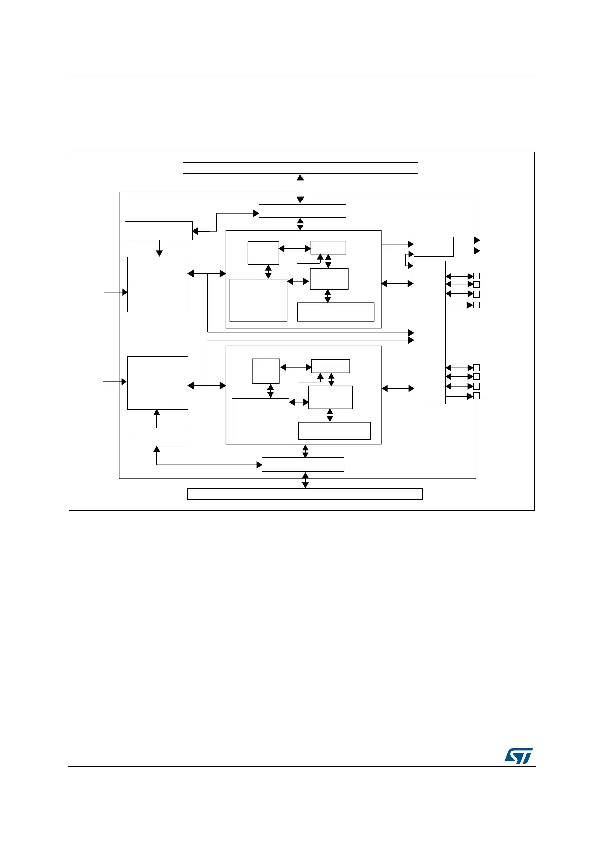
29.3 Functional block diagram
The block diagram of the SAI is shown in Figure 283.
Figure 283. Functional block diagram
The SAI is mainly composed of two audio sub-blocks with their own clock generator. Each
audio block integrates a 32-bit shift register controlled by their own functional state machine.
Data are stored or read from the dedicated FIFO. FIFO may be accessed by the CPU, or by
DMA in order to leave the CPU free during the communication. Each audio block is
independent. They can be synchronous with each other.
An I/O line controller manages each dedicated pins for a given audio block in the SAI. If the
two blocks are synchronized, this controller reduces the number of I/Os used, freeing up an
FS pin, an SCK pin and eventually an MCLK pin, making them general purpose I/Os.
The functional state machine can be configured to address a wide range of audio protocols.
Some registers are present to set-up the desired protocols (audio frame waveform
generator).
The audio block can be a transmitter or receiver, in master or slave mode. The master mode
means the bit clock SCK and the frame synchronization signal are generated from the SAI,
whereas in slave mode, they come from another external or internal master. There is a
particular case for which the FS signal direction is not directly linked to the master or slave
MS30032V1
FIFO
FIFO
Audio block A
32-bit shift register
APB interface
APB interface
Serial Audio Interface
FIFO ctrl
FSM
Configuration
registers and
Status register
APB
APB
SAI_CK_A
synchro
ctrl out
int_sck
int_FS
FS_A
SCK_A
SD_A
MCLK_A
SAI_XCR1
Clock generator
Audio block A
FSM
(SAI)
Audio block B
FIFO ctrl
Configuration
registers and
Status register
Clock generator
Audio block B
SAI_XCR1
SAI_CK_B
I/O line Management
FS_B
SCK_B
SD_B
MCLK_B
32-bit shift register