Analog-to-digital converter (ADC) RM0090
390/1749 RM0090 Rev 18
13.3.1 ADC on-off control
The ADC is powered on by setting the ADON bit in the ADC_CR2 register. When the ADON
bit is set for the first time, it wakes up the ADC from the Power-down mode.
Conversion starts when either the SWSTART or the JSWSTART bit is set.
You can stop conversion and put the ADC in power down mode by clearing the ADON bit. In
this mode the ADC consumes almost no power (only a few µA).
13.3.2 ADC clock
The ADC features two clock schemes:
• Clock for the analog circuitry: ADCCLK, common to all ADCs
This clock is generated from the APB2 clock divided by a programmable prescaler that
allows the ADC to work at f
PCLK2
/2, /4, /6 or /8. Refer to the datasheets for the
maximum value of ADCCLK.
• Clock for the digital interface (used for registers read/write access)
This clock is equal to the APB2 clock. The digital interface clock can be
enabled/disabled individually for each ADC through the RCC APB2 peripheral clock
enable register (RCC_APB2ENR).
13.3.3 Channel selection
There are 16 multiplexed channels. It is possible to organize the conversions in two groups:
regular and injected. A group consists of a sequence of conversions that can be done on
any channel and in any order. For instance, it is possible to implement the conversion
sequence in the following order: ADC_IN3, ADC_IN8, ADC_IN2, ADC_IN2, ADC_IN0,
ADC_IN2, ADC_IN2, ADC_IN15.
• A regular group is composed of up to 16 conversions. The regular channels and their
order in the conversion sequence must be selected in the ADC_SQRx registers. The
total number of conversions in the regular group must be written in the L[3:0] bits in the
ADC_SQR1 register.
• An injected group is composed of up to 4 conversions. The injected channels and
their order in the conversion sequence must be selected in the ADC_JSQR register.
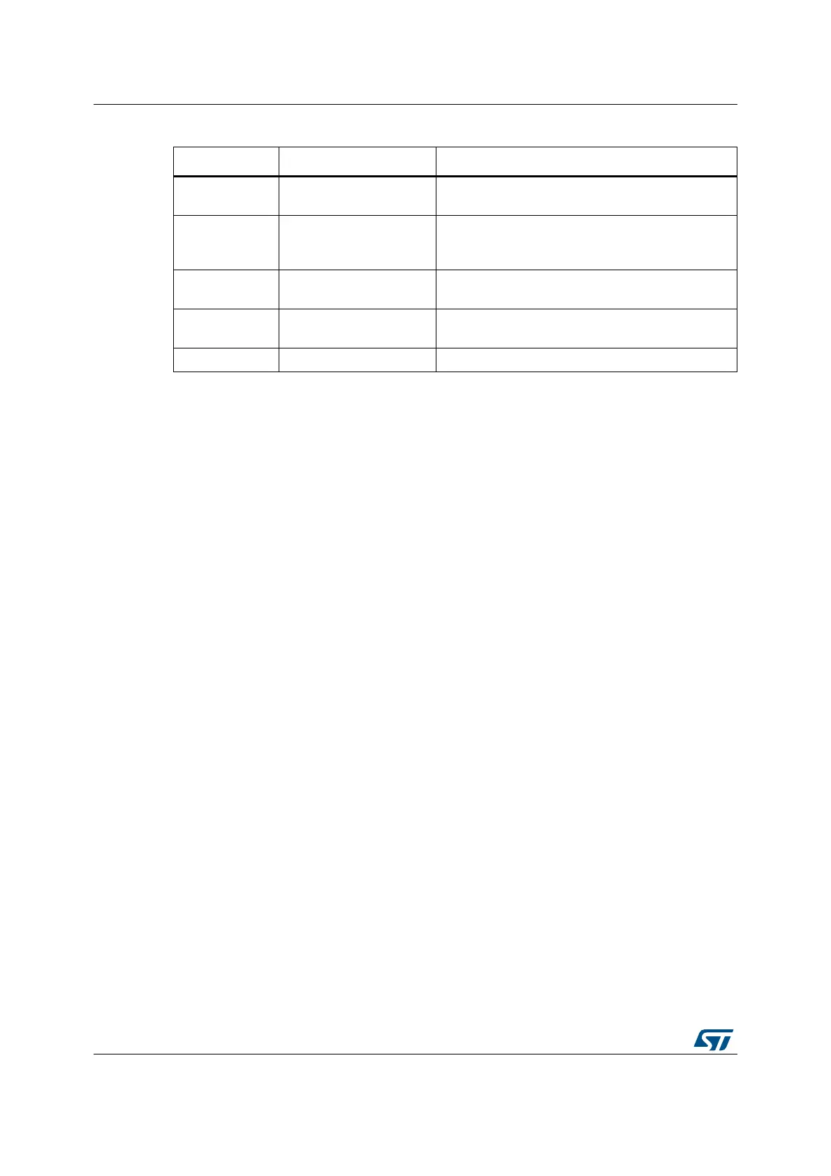
Table 65. ADC pins
Name Signal type Remarks
V
REF+
Input, analog reference
positive
The higher/positive reference voltage for the ADC,
1.8 V ≤ V
REF+
≤ V
DDA
V
DDA
Input, analog supply
Analog power supply equal to V
DD
and
2.4 V
≤ V
DDA
≤ V
DD
(3.6 V) for full speed
1.8 V ≤ V
DDA
≤ V
DD
(3.6 V) for reduced speed
V
REF–
Input, analog reference
negative
The lower/negative reference voltage for the ADC,
V
REF–
=
V
SSA
V
SSA
Input, analog supply
ground
Ground for analog power supply equal to V
SS
ADCx_IN[15:0] Analog input signals 16 analog input channels