RM0090 Rev 18 103/1749
RM0090 Embedded Flash memory interface
112
3.9.7 Flash control register (FLASH_CR) for
STM32F405xx/07xx and STM32F415xx/17xx
The Flash control register is used to configure and start Flash memory operations.
Address offset: 0x10
Reset value: 0x8000 0000
Access: no wait state when no Flash memory operation is ongoing, word, half-word and
byte access.
Bit 6 PGPERR: Programming parallelism error
Set by hardware when the size of the access (byte, half-word, word, double word) during the
program sequence does not correspond to the parallelism configuration PSIZE (x8, x16, x32,
x64).
Cleared by writing 1.
Bit 5 PGAERR: Programming alignment error
Set by hardware when the data to program cannot be contained in the same 128-bit Flash
memory row.
Cleared by writing 1.
Bit 4 WRPERR: Write protection error
Set by hardware when an address to be erased/programmed belongs to a write-protected part
of the Flash memory.
Cleared by writing 1.
Bits 3:2 Reserved, must be kept cleared.
Bit 1 OPERR: Operation error
Set by hardware when a flash operation (programming/erase/read) request is detected and
can not be run because of parallelism, alignment, write or read (PCROP) protection error. This
bit is set only if error interrupts are enabled (ERRIE = 1).
Bit 0 EOP: End of operation
Set by hardware when one or more Flash memory operations (program/erase) has/have
completed successfully. It is set only if the end of operation interrupts are enabled (EOPIE = 1).
Cleared by writing a 1.
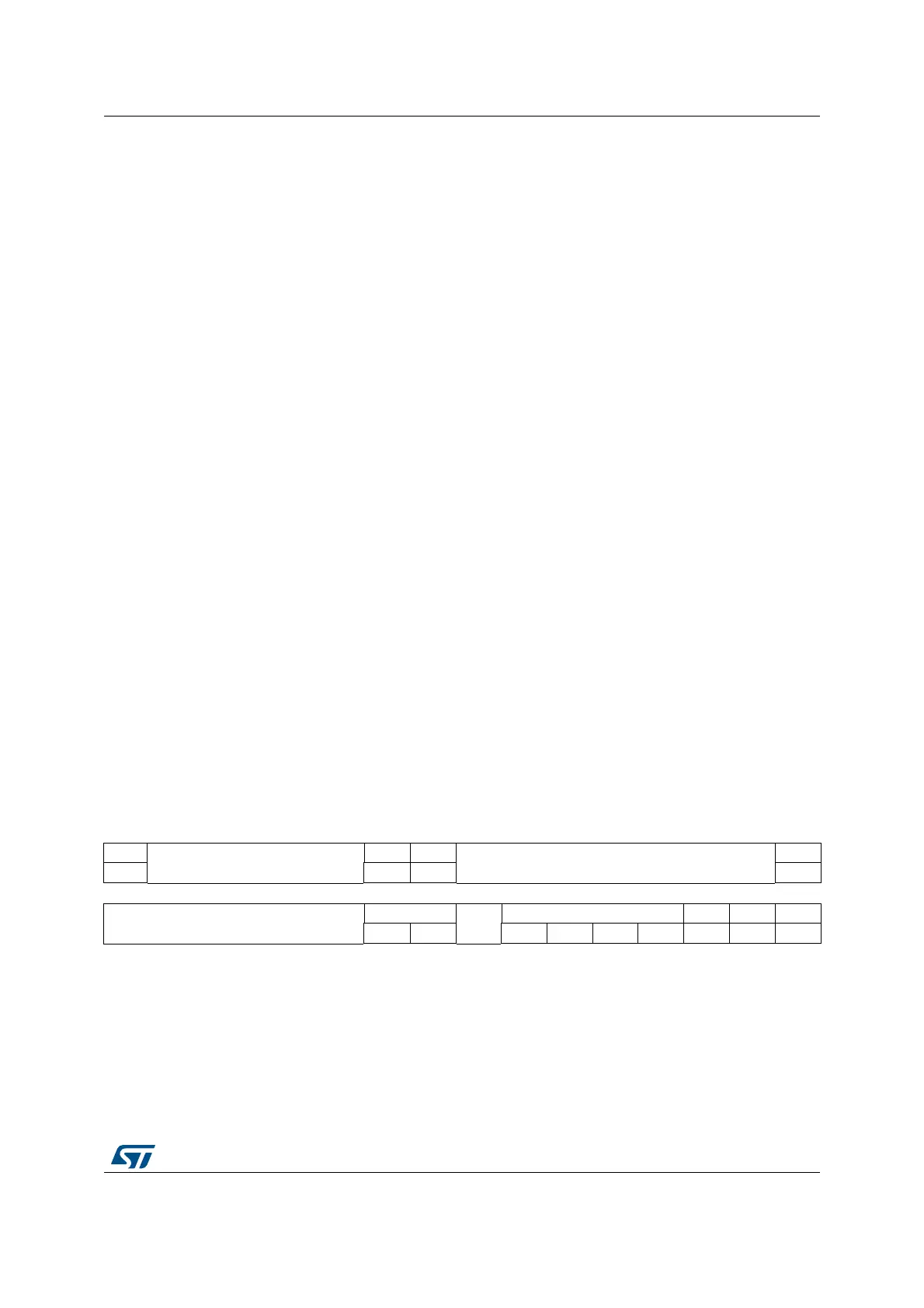
31 30 29 28 27 26 25 24 23 22 21 20 19 18 17 16
LOCK
Reserved
ERRIE EOPIE
Reserved
STRT
rs rw rw rs
15 14 13 12 11 10 9 8 7 6 5 4 3 2 1 0
Reserved
PSIZE[1:0]
Res.
SNB[3:0] MER SER PG
rw rw rw rw rw rw rw rw rw