Flexible static memory controller (FSMC) RM0090
1592/1749 RM0090 Rev 18
transfers at even addresses: nCE1 will be asserted low, NCE2 will be asserted high
and only the even bytes will be valid.
• Accesses to I/O Space can be performed either through AHB 8-bit or 16-bit accesses.
The FSMC Bank 4 gives access to those 3 memory spaces as described in Section 36.4.2:
NAND/PC Card address mapping and Table 218: Memory mapping and timing registers.
Wait Feature
The CompactFlash Storage or PC Card may request the FSMC to extend the length of the
access phase programmed by MEMWAITx/ATTWAITx/IOWAITx bits, asserting the nWAIT
signal after nOE/nWE or nIORD/nIOWR activation if the wait feature is enabled through the
PWAITEN bit in the FSMC_PCRx register. In order to detect the nWAIT assertion correctly,
the MEMWAITx/ATTWAITx/IOWAITx bits must be programmed as follows:
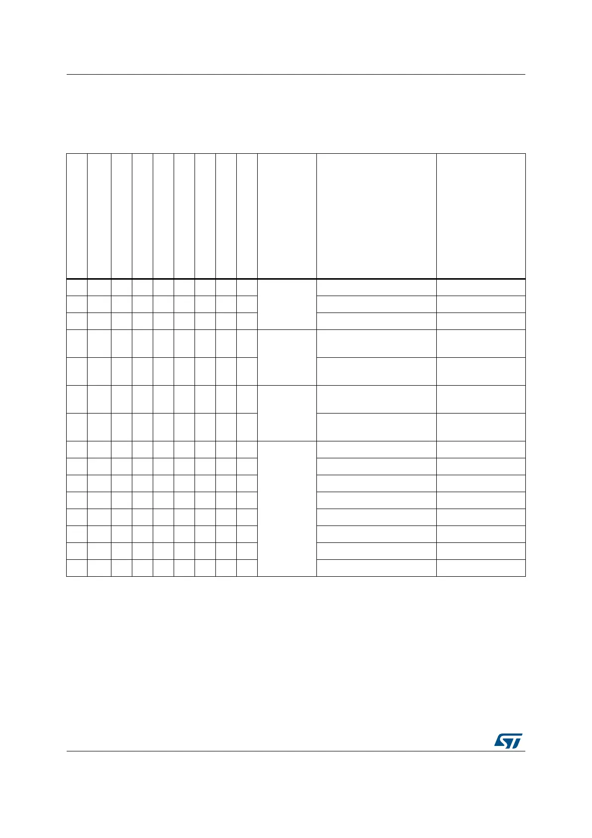
Table 251. 16-bit PC-Card signals and access type
nCE2
nCE1
nREG
nOE/nWE
nIORD /nIOWR
A10
A9
A7-1
A0
Space Access Type
Allowed/not
Allowed
1 0 101XXX-XX
Common
Memory
Space
Read/Write byte on D7-D0 YES
0 1 1 0 1 X X X-X X Read/Write byte on D15-D8 Not supported
0 0 1 0 1 X X X-X 0 Read/Write word on D15-D0 YES
X0 00101X-X0
Attribute
Space
Read or Write Configuration
Registers
YES
X0 00100X-X0
Read or Write CIS (Card
Information Structure)
YES
1 0 001XXX-X1
Attribute
Space
Invalid Read or Write (odd
address)
YES
0 1 001XXX-Xx
Invalid Read or Write (odd
address)
YES
1 0 010XXX-X0
I/O space
Read Even Byte on D7-0 YES
1 0 0 1 0 X X X-X 1 Read Odd Byte on D7-0 YES
1 0 0 1 0 X X X-X 0 Write Even Byte on D7-0 YES
1 0 0 1 0 X X X-X 1 Write Odd Byte on D7-0 YES
0 0 0 1 0 X X X-X 0 Read Word on D15-0 YES
0 0 0 1 0 X X X-X 0 Write word on D15-0 YES
0 1 0 1 0 X X X-X X Read Odd Byte on D15-8 Not supported
0 1 0 1 0 X X X-X X Write Odd Byte on D15-8 Not supported