RM0090 Rev 18 845/1749
RM0090 Inter-integrated circuit (I2C) interface
872
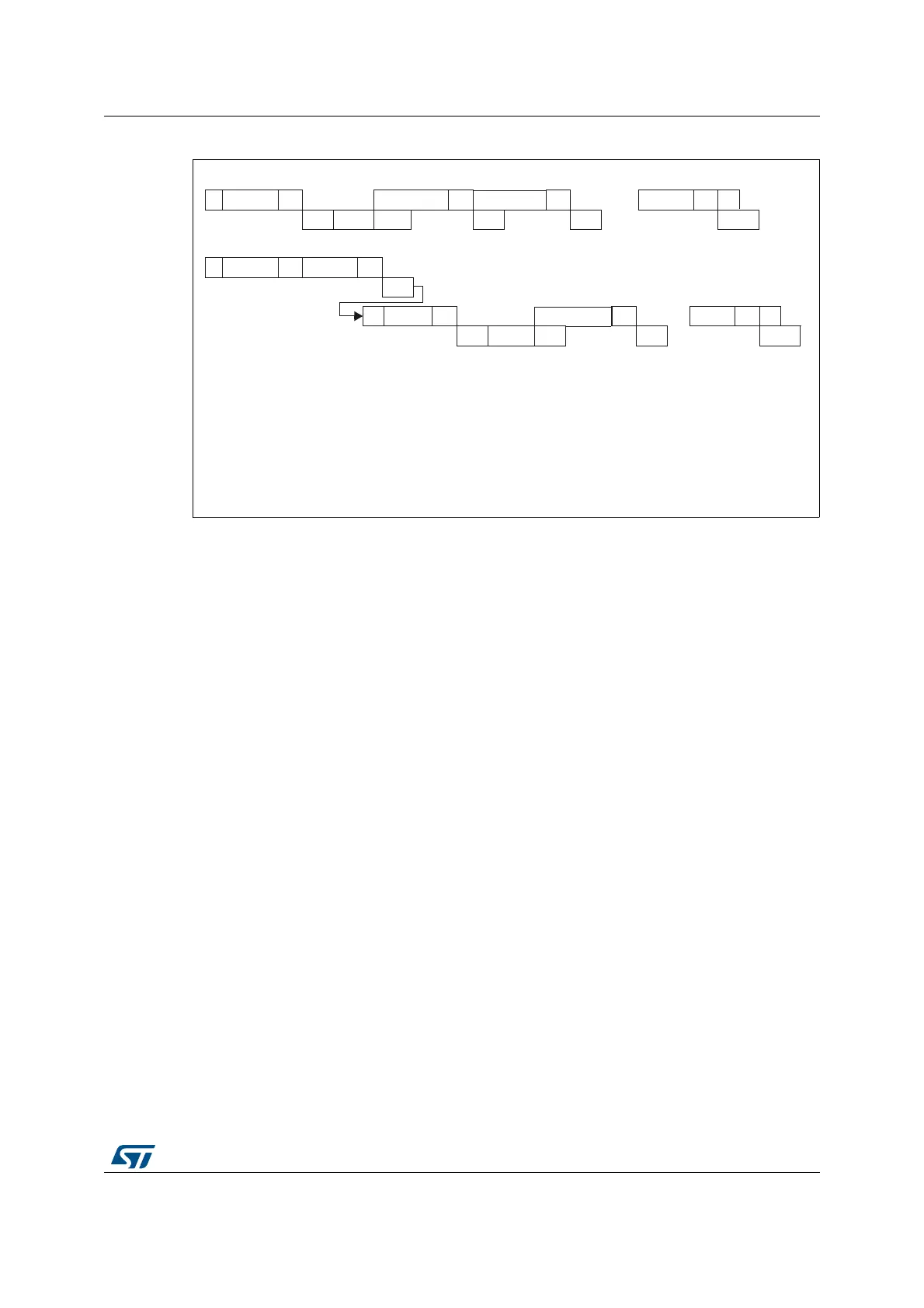
Figure 241. Transfer sequence diagram for slave transmitter
1. The EV1 and EV3_1 events stretch SCL low until the end of the corresponding software sequence.
2. The EV3 event stretches SCL low if the software sequence is not completed before the end of the next byte
transmission.
Slave receiver
Following the address reception and after clearing ADDR, the slave receives bytes from the
SDA line into the DR register via the internal shift register. After each byte the interface
generates in sequence:
• An acknowledge pulse if the ACK bit is set
• The RxNE bit is set by hardware and an interrupt is generated if the ITEVFEN and
ITBUFEN bit is set.
If RxNE is set and the data in the DR register is not read before the end of the next data
reception, the BTF bit is set and the interface waits until BTF is cleared by a read from the
I2C_DR register, stretching SCL low (see Figure 242 Transfer sequencing).
7-bit slave transmitter
10-bit slave transmitter
Legend: S= Start, S
r
= Repeated Start, P= Stop, A= Acknowledge, NA= Non-acknowledge,
EVx= Event (with interrupt if ITEVFEN=1)
EV1: ADDR=1, cleared by reading SR1 followed by reading SR2
EV3-1: TxE=1, shift register empty, data register empty, write Data1 in DR.
EV3: TxE=1, shift register not empty, data register empty, cleared by writing DR
EV3-2: AF=1; AF is cleared by writing ‘0’ in AF bit of SR1 register.
S Address A Data1 A Data2 A
.....
DataN NA P
EV1 EV3-1 EV3 EV3 EV3 EV3-2
S Header A Address A
EV1
S
r
Header A Data1 A
....
DataN NA
P
EV1 EV3_1 EV3 EV3 EV3-2
ai18209