RM0090 Rev 18 545/1749
RM0090 Advanced-control timers (TIM1 and TIM8)
588
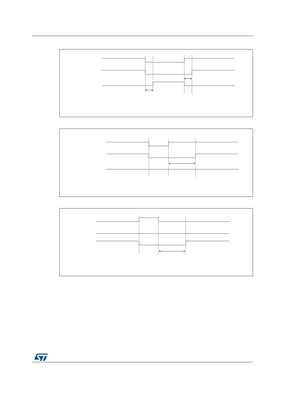
Figure 120. Complementary output with dead-time insertion.
Figure 121. Dead-time waveforms with delay greater than the negative pulse.
Figure 122. Dead-time waveforms with delay greater than the positive pulse.
The dead-time delay is the same for each of the channels and is programmable with the
DTG bits in the TIMx_BDTR register. Refer to Section 17.4.18: TIM1 and TIM8 break and
dead-time register (TIMx_BDTR) for delay calculation.
Re-directing OCxREF to OCx or OCxN
In output mode (forced, output compare or PWM), OCxREF can be re-directed to the OCx
output or to OCxN output by configuring the CCxE and CCxNE bits in the TIMx_CCER
register.
This allows the user to send a specific waveform (such as PWM or static active level) on
one output while the complementary remains at its inactive level. Other possibilities are to
delay
delay
OCxREF
OCx
OCxN
MS31095V1
MS31096V1
delay
OCxREF
OCx
OCxN
MS31097V1
delay
OCxREF
OCx
OCxN