Analog-to-digital converter (ADC) RM0090
430/1749 RM0090 Rev 18
13.13.17 ADC common regular data register for dual and triple modes
(ADC_CDR)
Address offset: 0x08 (this offset address is relative to ADC1 base address + 0x300)
Reset value: 0x0000 0000
13.13.18 ADC register map
The following table summarizes the ADC registers.
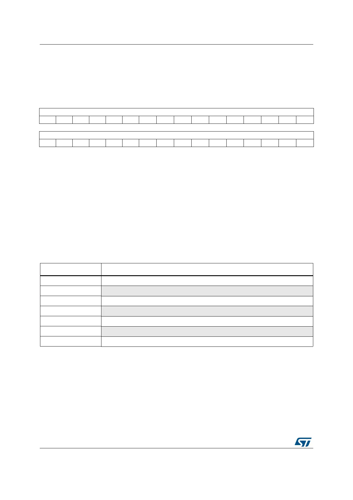
31 30 29 28 27 26 25 24 23 22 21 20 19 18 17 16
DATA2[15:0]
rrrrrr r r r r rrrrrr
1514131211109876543210
DATA1[15:0]
rrrrrr r r r r rrrrrr
Bits 31:16 DATA2[15:0]: 2nd data item of a pair of regular conversions
– In dual mode, these bits contain the regular data of ADC2. Refer to Dual ADC mode.
– In triple mode, these bits contain alternatively the regular data of ADC2, ADC1 and ADC3.
Refer to Triple ADC mode.
Bits 15:0 DATA1[15:0]: 1st data item of a pair of regular conversions
– In dual mode, these bits contain the regular data of ADC1. Refer to Dual ADC mode
– In triple mode, these bits contain alternatively the regular data of ADC1, ADC3 and ADC2.
Refer to Triple ADC mode.
Table 71. ADC global register map
Offset Register
0x000 - 0x04C ADC1
0x050 - 0x0FC
Reserved
0x100 - 0x14C ADC2
0x118 - 0x1FC
Reserved
0x200 - 0x24C ADC3
0x250 - 0x2FC
Reserved
0x300 - 0x308 Common registers