Inter-integrated circuit (I2C) interface RM0090
846/1749 RM0090 Rev 18
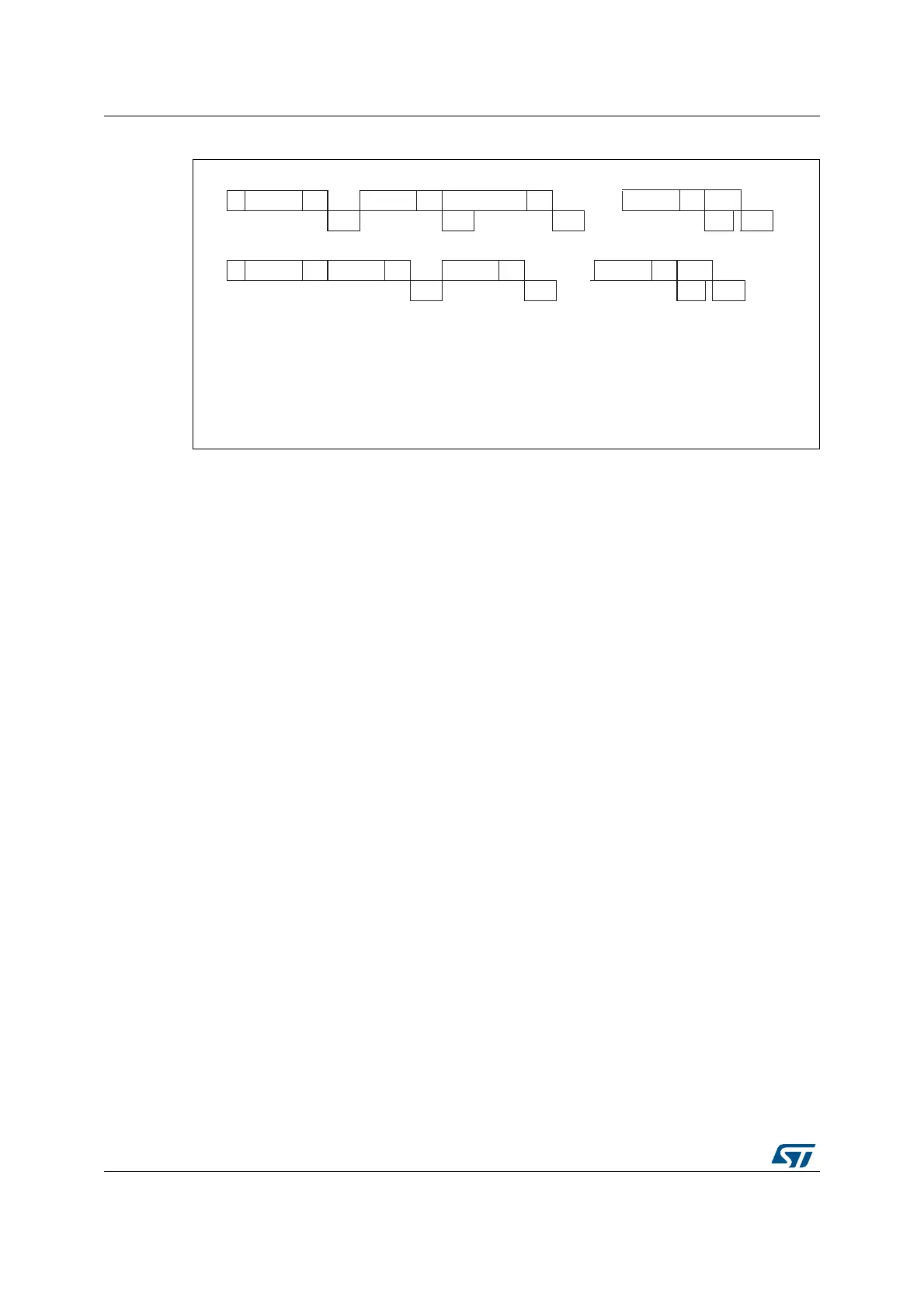
Figure 242. Transfer sequence diagram for slave receiver
1. The EV1 event stretches SCL low until the end of the corresponding software sequence.
2. The EV2 event stretches SCL low if the software sequence is not completed before the end of the next byte
reception.
3. After checking the SR1 register content, the user should perform the complete clearing sequence for each
flag found set.
Thus, for ADDR and STOPF flags, the following sequence is required inside the I2C interrupt routine:
READ SR1
if (ADDR == 1) {READ SR1; READ SR2}
if (STOPF == 1) {READ SR1; WRITE CR1}
The purpose is to make sure that both ADDR and STOPF flags are cleared if both are found set.
Closing slave communication
After the last data byte is transferred a Stop Condition is generated by the master. The
interface detects this condition and sets:
• The STOPF bit and generates an interrupt if the ITEVFEN bit is set.
The STOPF bit is cleared by a read of the SR1 register followed by a write to the CR1
register (see EV4 in Figure 242).
27.3.3 I
2
C master mode
In Master mode, the I
2
C interface initiates a data transfer and generates the clock signal. A
serial data transfer always begins with a Start condition and ends with a Stop condition.
Master mode is selected as soon as the Start condition is generated on the bus with a
START bit.
The following is the required sequence in master mode.
• Program the peripheral input clock in I2C_CR2 Register in order to generate correct
timings
• Configure the clock control registers
• Configure the rise time register
• Program the I2C_CR1 register to enable the peripheral
• Set the START bit in the I2C_CR1 register to generate a Start condition
The peripheral input clock frequency must be at least:
• 2 MHz in Sm mode
• 4 MHz in Fm mode
7-bit slave receiver
10-bit slave receiver
Legend: S= Start, S
r
= Repeated Start, P= Stop, A= Acknowledge,
EVx= Event (with interrupt if ITEVFEN=1)
EV1: ADDR=1, cleared by reading SR1 followed by reading SR2
EV2: RxNE=1 cleared by reading DR register.
EV4: STOPF=1, cleared by reading SR1 register followed by writing to the CR1 register
S Address A Data1 A Data2 A
.....
DataN A
P
EV1 EV2 EV2 EV2 EV4
S Header A Address A Data1 A
.....
DataN A P
EV1 EV2 EV2
EV4
ai18208