Embedded Flash memory interface RM0090
94/1749 RM0090 Rev 18
--
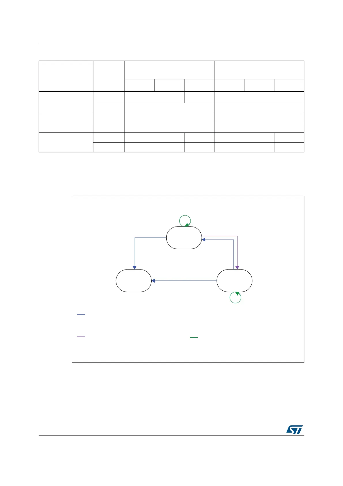
Figure 6 shows how to go from one RDP level to another.
Figure 6. RDP levels
3.7.4 Write protections
Up to 24 user sectors in Flash memory can be protected against unwanted write operations
due to loss of program counter contexts. When the non-write protection nWRPi bit (0 ≤i ≤11)
in the FLASH_OPTCR or FLASH_OPTCR1 registers is low, the corresponding sector
Table 17. Access versus read protection level
Memory area
Protection
Level
Debug features, Boot from RAM or
from System memory bootloader
Booting from Flash memory
Read Write Erase Read Write Erase
Main Flash Memory
and Backup SRAM
Level 1 NO NO
(1)
YES
Level 2 NO YES
Option Bytes
Level 1 YES YES
Level 2 NO NO
OTP
Level 1 NO NA YES NA
Level 2 NO NA YES NA
1. The main Flash memory and backup SRAM are only erased when the RDP changes from level 1 to 0. The OTP area
remains unchanged.
Level 1
RDP /= AAh
RDP /= CCh
default
Options write (RDP level increase) includes
- Options erase
- New options program
Options write (RDP level decrease) includes
- Mass erase
- Options erase
- New options program
Options write (RDP level identical) includes
- Options erase
- New options program
RDP = AAh
Others option(s) modified
RDP /= AAh & /= CCh
Others options modified
Write options
including
RDP = AAh
Write options
including
RDP = CCh
Write options
including
RDP = CCh
Write options including
RDP /= CCh & /= AAh
Level 2
RDP = CCh
Level 0
RDP = AAh
MS47541V1