RM0090 Rev 18 1407/1749
RM0090 USB on-the-go high-speed (OTG_HS)
1543
Data FIFO (DFIFO) access register map
These registers, available in both host and peripheral modes, are used to read or write the
FIFO space for a specific endpoint or a channel, in a given direction. If a host channel is of
type IN, the FIFO can only be read on the channel. Similarly, if a host channel is of type
OUT, the FIFO can only be written on the channel.
Power and clock gating CSR map
There is a single register for power and clock gating. It is available in both host and
peripheral modes.
35.12.2 OTG_HS global registers
These registers are available in both host and peripheral modes, and do not need to be
reprogrammed when switching between these modes.
OTG_HS_DOEPINTx
0xB08
0xB28
...
0xBA8
OTG_HS device endpoint-x interrupt register
(OTG_HS_DOEPINTx) (x = 0..5, where x = Endpoint_number) on
page 1466
OTG_HS_DOEPTSIZx
0xB30
0xB50
...
0xBB0
OTG_HS device endpoint-x transfer size register
(OTG_HS_DOEPTSIZx) (x = 1..5, where x = Endpoint_number)
on page 1470
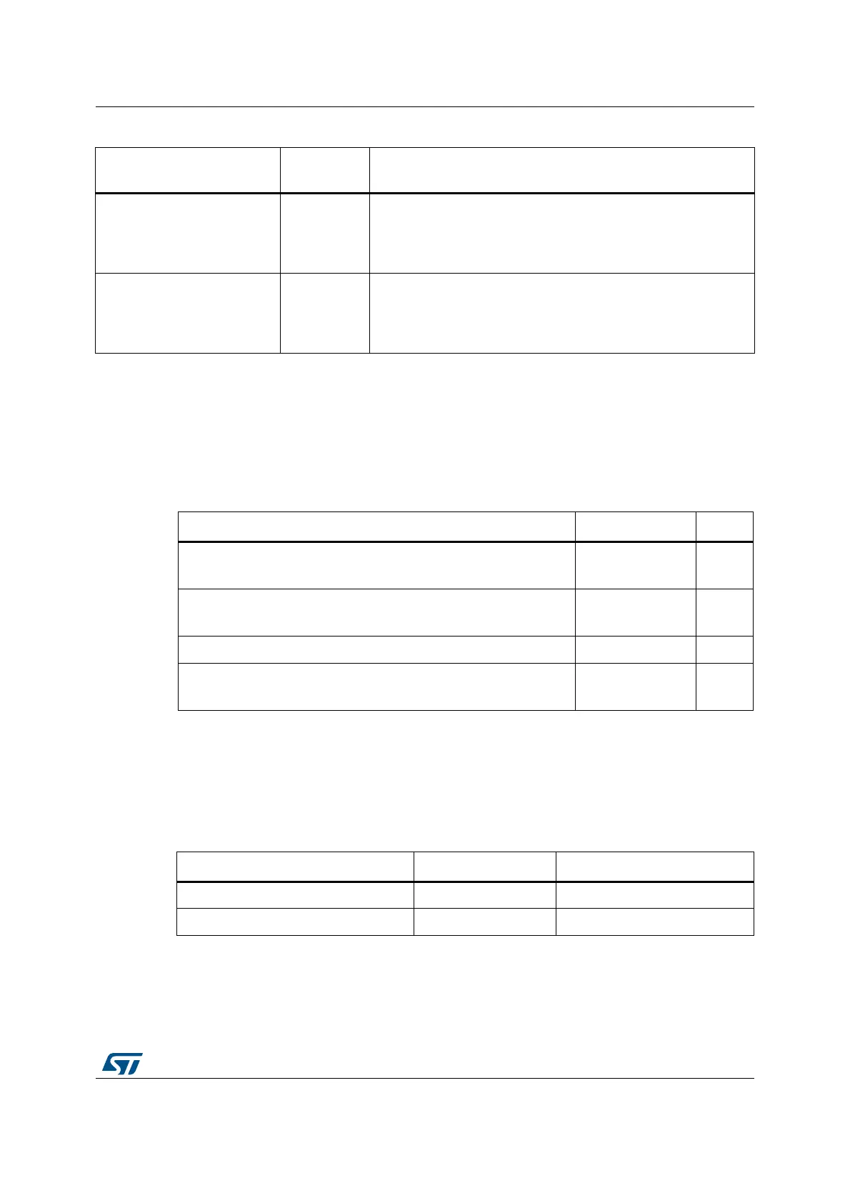
Table 210. Device-mode control and status registers (continued)
Acronym
Offset
address
Register name
Table 211. Data FIFO (DFIFO) access register map
FIFO access register section Address range Access
Device IN Endpoint 0/Host OUT Channel 0: DFIFO Write Access
Device OUT Endpoint 0/Host IN Channel 0: DFIFO Read Access
0x1000–0x1FFC
w
r
Device IN Endpoint 1/Host OUT Channel 1: DFIFO Write Access
Device OUT Endpoint 1/Host IN Channel 1: DFIFO Read Access
0x2000–0x2FFC
w
r
... ... ...
Device IN Endpoint x
(1)
/Host OUT Channel x
(1)
: DFIFO Write Access
Device OUT Endpoint x
(1)
/Host IN Channel x
(1)
: DFIFO Read Access
1. Where x is 5 in peripheral mode and 11 in host mode.
0xX000–0xXFFC
w
r
Table 212. Power and clock gating control and status registers
Register name Acronym Offset address: 0xE00–0xFFF
Power and clock gating control register OTG_HS_PCGCCTL 0xE00-0xE04
Reserved - 0xE05–0xFFF