RM0090 Rev 18 263/1749
RM0090 Reset and clock control for STM32F405xx/07xx and STM32F415xx/17xx(RCC)
266
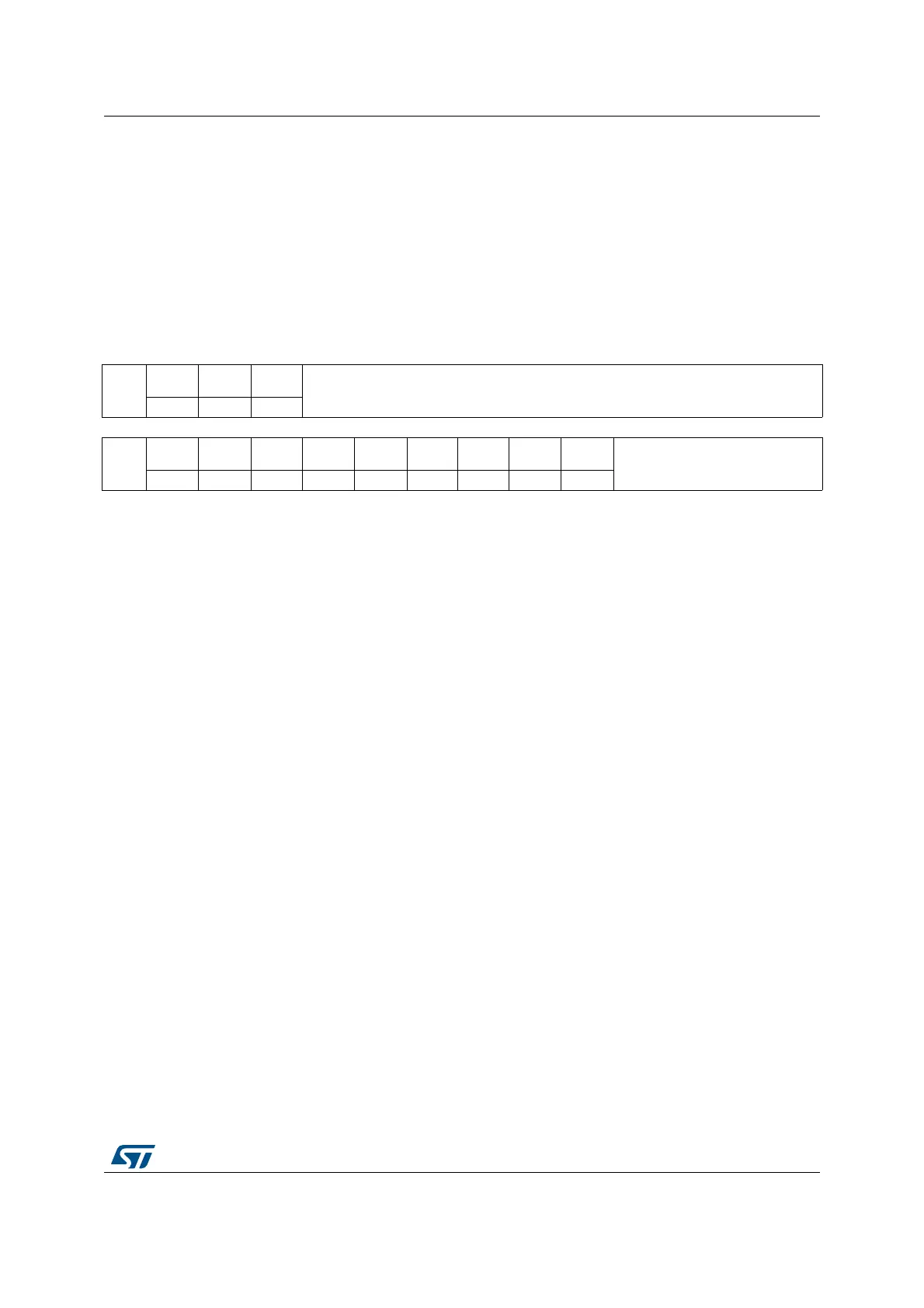
7.3.23 RCC PLLI2S configuration register (RCC_PLLI2SCFGR)
Address offset: 0x84
Reset value: 0x2000 3000
Access: no wait state, word, half-word and byte access.
This register is used to configure the PLLI2S clock outputs according to the formulas:
• f
(VCO clock)
= f
(PLLI2S clock input)
× (PLLI2SN / PLLM)
• f
(PLL I2S clock output)
= f
(VCO clock)
/ PLLI2SR
31 30 29 28 27 26 25 24 23 22 21 20 19 18 17 16
Reserv
ed
PLLI2S
R2
PLLI2S
R1
PLLI2S
R0
Reserved
rw rw rw
15 14 13 12 11 10 9 8 7 6 5 4 3 2 1 0
Reserv
ed
PLLI2SN
8
PLLI2SN
7
PLLI2SN
6
PLLI2SN
5
PLLI2SN
4
PLLI2SN
3
PLLI2SN
2
PLLI2SN
1
PLLI2SN
0
Reserved
rw rw rw rw rw rw rw rw rw
Bit 31 Reserved, must be kept at reset value.
Bits 30:28 PLLI2SR: PLLI2S division factor for I2S clocks
Set and cleared by software to control the I2S clock frequency. These bits should be written
only if the PLLI2S is disabled. The factor must be chosen in accordance with the prescaler
values inside the I2S peripherals, to reach 0.3% error when using standard crystals and 0%
error with audio crystals. For more information about I2S clock frequency and precision,
refer to Section 28.4.4: Clock generator in the I2S chapter.
Caution: The I2Ss requires a frequency lower than or equal to 192 MHz to work correctly.
I2S clock frequency = VCO frequency / PLLR with 2 ≤ PLLR ≤ 7
000: PLLR = 0, wrong configuration
001: PLLR = 1, wrong configuration
010: PLLR = 2
...
111: PLLR = 7