RM0090 Rev 18 407/1749
RM0090 Analog-to-digital converter (ADC)
432
13.9.3 Interleaved mode
This mode can be started only on a regular group (usually one channel). The external
trigger source comes from the regular channel multiplexer of ADC1.
Dual ADC mode
After an external trigger occurs:
• ADC1 starts immediately
• ADC2 starts after a delay of several
ADC clock cycles
The minimum delay which separates 2 conversions in interleaved mode is configured in the
DELAY bits in the ADC_CCR register. However, an ADC cannot start a conversion if the
complementary ADC is still sampling its input (only one ADC can sample the input signal at
a given time). In this case, the delay becomes the sampling time + 2 ADC clock cycles. For
instance, if DELAY = 5 clock cycles and the sampling takes 15 clock cycles on both ADCs,
then 17 clock cycles will separate conversions on ADC1 and ADC2).
If the CONT bit is set on both ADC1 and ADC2, the selected regular channels of both ADCs
are continuously converted.
Note: If the conversion sequence is interrupted (for instance when DMA end of transfer occurs),
the multi-ADC sequencer must be reset by configuring it in independent mode first (bits
DUAL[4:0] = 00000) before reprogramming the interleaved mode.
After an EOC interrupt is generated by ADC2 (if enabled through the EOCIE bit) a 32-bit
DMA transfer request is generated (if the DMA[1:0] bits in ADC_CCR are equal to 0b10).
This request first transfers the ADC2 converted data stored in the upper half-word of the
ADC_CDR 32-bit register into SRAM, then the ADC1 converted data stored in the register’s
lower half-word into SRAM.
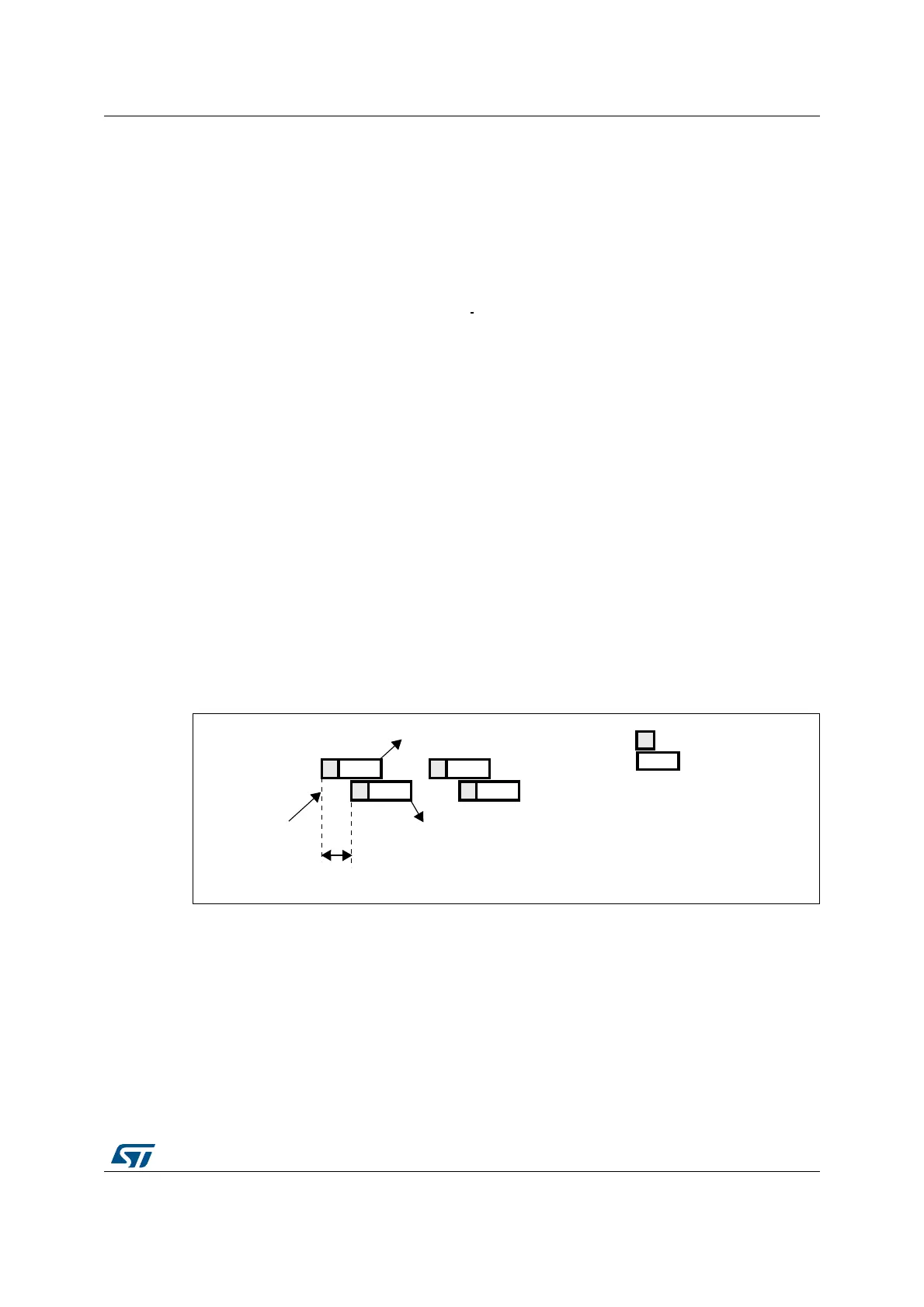
Figure 56. Interleaved mode on 1 channel in continuous conversion mode: dual ADC
mode
Triple ADC mode
After an external trigger occurs:
• ADC1 starts immediately and
• ADC2 starts after a delay of several ADC clock cycles
• ADC3 starts after a delay of several ADC clock cycles referred to the ADC2 conversion
The minimum delay which separates 2 conversions in interleaved mode is configured in the
DELAY bits in the ADC_CCR register. However, an ADC cannot start a conversion if the
complementary ADC is still sampling its input (only one ADC can sample the input signal at
CH0
CH0
ADC1
ADC2
Trigger
End of conversion on ADC2
CH0
CH0
...
...
8 ADCCLK
cycles
End of conversion on ADC1
Conversion
Sampling
ai16056