Flexible memory controller (FMC) RM0090
1666/1749 RM0090 Rev 18
SDRAM controller read cycle
The SDRAM controller accepts single and burst read requests and translates them into
single memory accesses. In both cases, the SDRAM controller keeps track of the active row
in each bank to be able to perform consecutive read accesses in different banks (Multibank
ping-pong access).
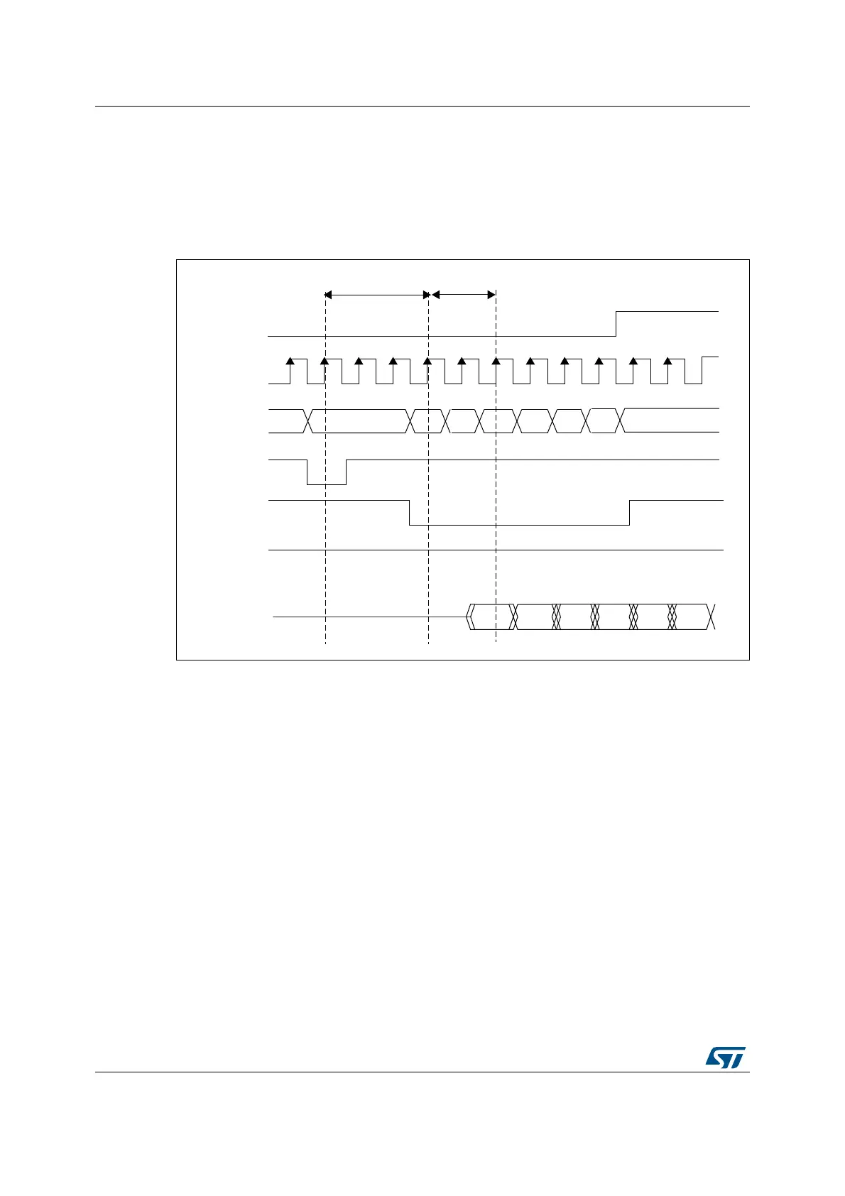
Figure 479. Burst read SDRAM access
The FMC SDRAM controller features a Cacheable read FIFO (6 lines x 32 bits). It is used to
store data read in advance during the CAS latency period and during the RPIPE delay. The
following the formula is applied:
The RBURST bit must be set in the FMC_SDCR1 register to anticipate the next read
access.
Example:
• CAS latency = 3, RPIPE delay = 0: 4 data (not committed) are stored in the FIFO.
• CAS latency = 3, RPIPE delay = 2: 5 data (not committed) are stored in the FIFO.
The read FIFO features a 14-bit address tag to each line to identify its content: 11 bits for the
column address, 2 bits to select the internal bank and the active row, and 1 bit to select the
SDRAM device
When the end of the row is reached in advance during an AHB burst read, the data read in
advance (not committed) are not stored in the read FIFO. For single read access, data are
correctly stored in the FIFO.
MS30449V3
NRAS
A[12:0]
SDCLK
Row n Colc
SDNE
TRCD = 3
NWE
Cola Cold
Colb Cole
Colf
NCAS
DATA[31:0]
Dnc DneDna Dnf
Dnb Dnd
CAS latency = 2
Number of anticipated data CAS latency 1 RPIPE delay()2⁄++=