RM0090 Rev 18 203/1749
RM0090 Reset and clock control for STM32F42xxx and STM32F43xxx (RCC)
212
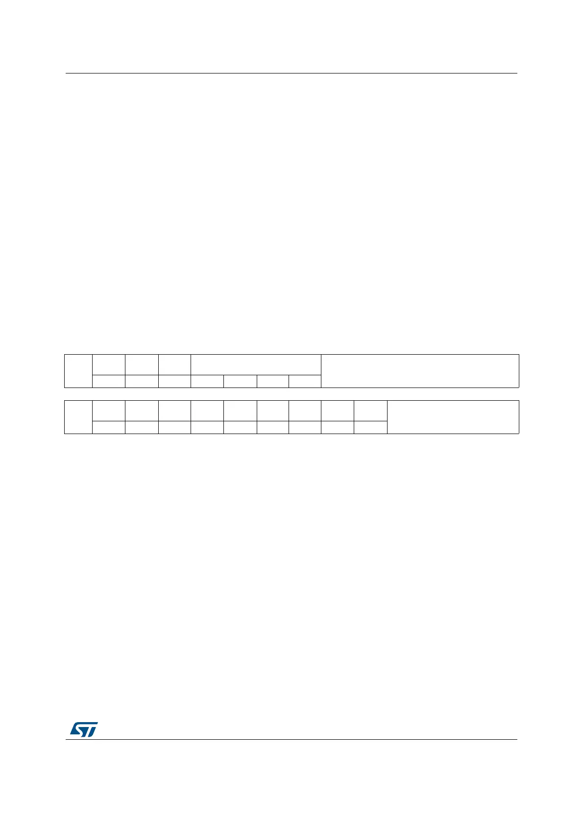
6.3.23 RCC PLLI2S configuration register (RCC_PLLI2SCFGR)
Address offset: 0x84
Reset value: 0x2400 3000
Access: no wait state, word, half-word and byte access.
This register is used to configure the PLLI2S clock outputs according to the formulas:
f
(VCO clock)
= f
(PLLI2S clock input)
× (PLLI2SN / PLLM)
f
(PLL I2S clock output)
= f
(VCO clock)
/ PLLI2SR
Bits 29:28 Reserved, must be kept at reset value.
Bits 27:13 INCSTEP: Incrementation step
These bits are set and cleared by software. To write before setting CR[24]=PLLON bit.
Configuration input for modulation profile amplitude.
Bits 12:0 MODPER: Modulation period
These bits are set and cleared by software. To write before setting CR[24]=PLLON bit.
Configuration input for modulation profile period.
31 30 29 28 27 26 25 24 23 22 21 20 19 18 17 16
Reserv
ed
PLLI2S
R2
PLLI2S
R1
PLLI2S
R0
PLLI2SQ
Reserved
rw rw rw rw rw rw rw
15 14 13 12 11 10 9 8 7 6 5 4 3 2 1 0
Reserv
ed
PLLI2SN
8
PLLI2SN
7
PLLI2SN
6
PLLI2SN
5
PLLI2SN
4
PLLI2SN
3
PLLI2SN
2
PLLI2SN
1
PLLI2SN
0
Reserved
rw rw rw rw rw rw rw rw rw