RM0090 Rev 18 457/1749
RM0090 Digital camera interface (DCMI)
479
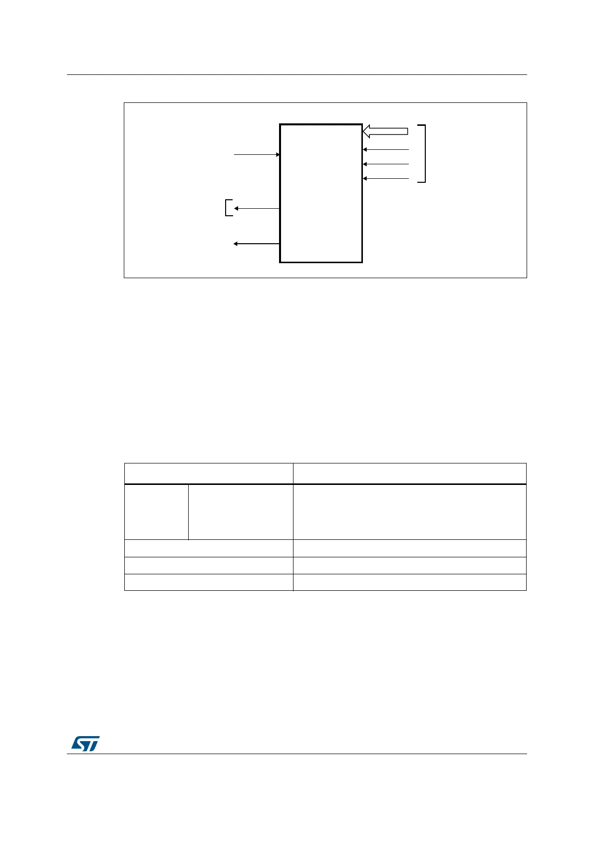
Figure 73. Top-level block diagram
15.5.1 DMA interface
The DMA interface is active when the CAPTURE bit in the DCMI_CR register is set. A DMA
request is generated each time the camera interface receives a complete 32-bit data block
in its register.
15.5.2 DCMI physical interface
The interface is composed of 11/13/15/17 inputs. Only the Slave mode is supported.
The camera interface can capture 8-bit, 10-bit, 12-bit or 14-bit data depending on the
EDM[1:0] bits in the DCMI_CR register. If less than 14 bits are used, the unused data pins
must not be assigned to DCMI interface through GPIO alternate functions.
The data are synchronous with PIXCLK and change on the rising/falling edge of the pixel
clock depending on the polarity.
The HSYNC signal indicates the start/end of a line.
The VSYNC signal indicates the start/end of a frame
DCMI
Interrupt
controller
DCMI_IT
External
interface
DCMI_D[0:13]
DCMI_PIXCLK
DCMI_HSYNC
DCMI_VSYNC
DMA_REQ
HCLK
ai15603b
Table 78. DCMI signals
Signal name Signal description
8 bits
10 bits
12 bits
14 bits
D[0..7]
D[0..9]
D[0..11]
D[0..13]
Data
PIXCLK Pixel clock
HSYNC Horizontal synchronization / Data valid
VSYNC Vertical synchronization