Digital-to-analog converter (DAC) RM0090
434/1749 RM0090 Rev 18
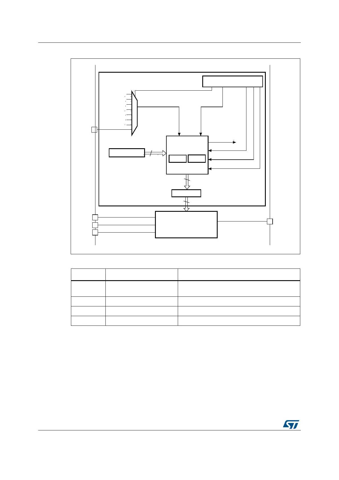
Figure 64. DAC channel block diagram
Note: Once the DAC channelx is enabled, the corresponding GPIO pin (PA4 or PA5) is
automatically connected to the analog converter output (DAC_OUTx). In order to avoid
parasitic consumption, the PA4 or PA5 pin should first be configured to analog (AIN).
Table 74. DAC pins
Name Signal type Remarks
V
REF+
Input, analog reference
positive
The higher/positive reference voltage for the DAC,
1.8 V
≤ V
REF+
≤ V
DDA
V
DDA
Input, analog supply Analog power supply
V
SSA
Input, analog supply ground Ground for analog power supply
DAC_OUTx Analog output signal DAC channelx analog output
V
DDA
V
SSA
V
REF+
DAC_ OUTx
Control logicx
DHRx
12-bit
12-bit
LFSRx
trianglex
DM A req ue stx
TSELx[2:0] bits
TIM4_T RGO
TIM5_T RGO
TIM6_T RGO
TIM7_T RGO
TIM2_T RGO
TIM8_T RGO
EXTI_9
DMAENx
TENx
MAMPx[3:0] bits
WAVENx[1:0] bits
SWTRIGx
DORx
Digital-to-analog
converterx
12-bit
DAC control register
ai14708b
Trigger selectorx