Flexible memory controller (FMC) RM0090
1638/1749 RM0090 Rev 18
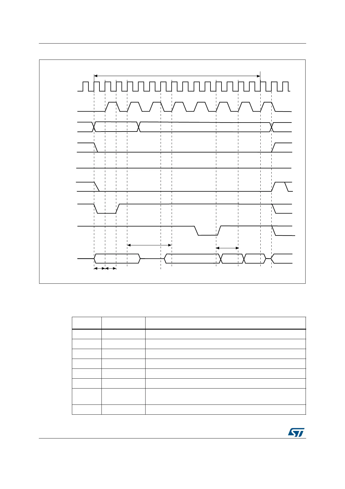
Figure 475. Synchronous multiplexed write mode waveforms - PSRAM (CRAM)
1. The memory must issue NWAIT signal one cycle in advance, accordingly WAITCFG must be programmed
to 0.
2. Byte Lane (NBL) outputs are not shown, they are held low while NEx is active.
Addr[15:0] data
addr[25:16]
Memory transaction = burst of 2 half words
HCLK
CLK
A[25:16]
NEx
NOE
NWE
Hi-Z
NADV
NWAIT
(WAITCFG = 0)
A/D[15:0]
1 clock 1 clock
(DATLAT + 2)
inserted wait state
ai14731f
CLK cycles
data
Table 287. FMC_BCRx bit fields
Bit No. Bit name Value to set
31-20 Reserved 0x000
20 CCLKEN As needed
19 CBURSTRW 0x1
18-16 CPSIZE As needed (0x1 for CRAM 1.5)
15 ASYNCWAIT 0x0
14 EXTMOD 0x0
13 WAITEN
to be set to 1 if the memory supports this feature, to be kept at 0
otherwise.
12 WREN 0x1