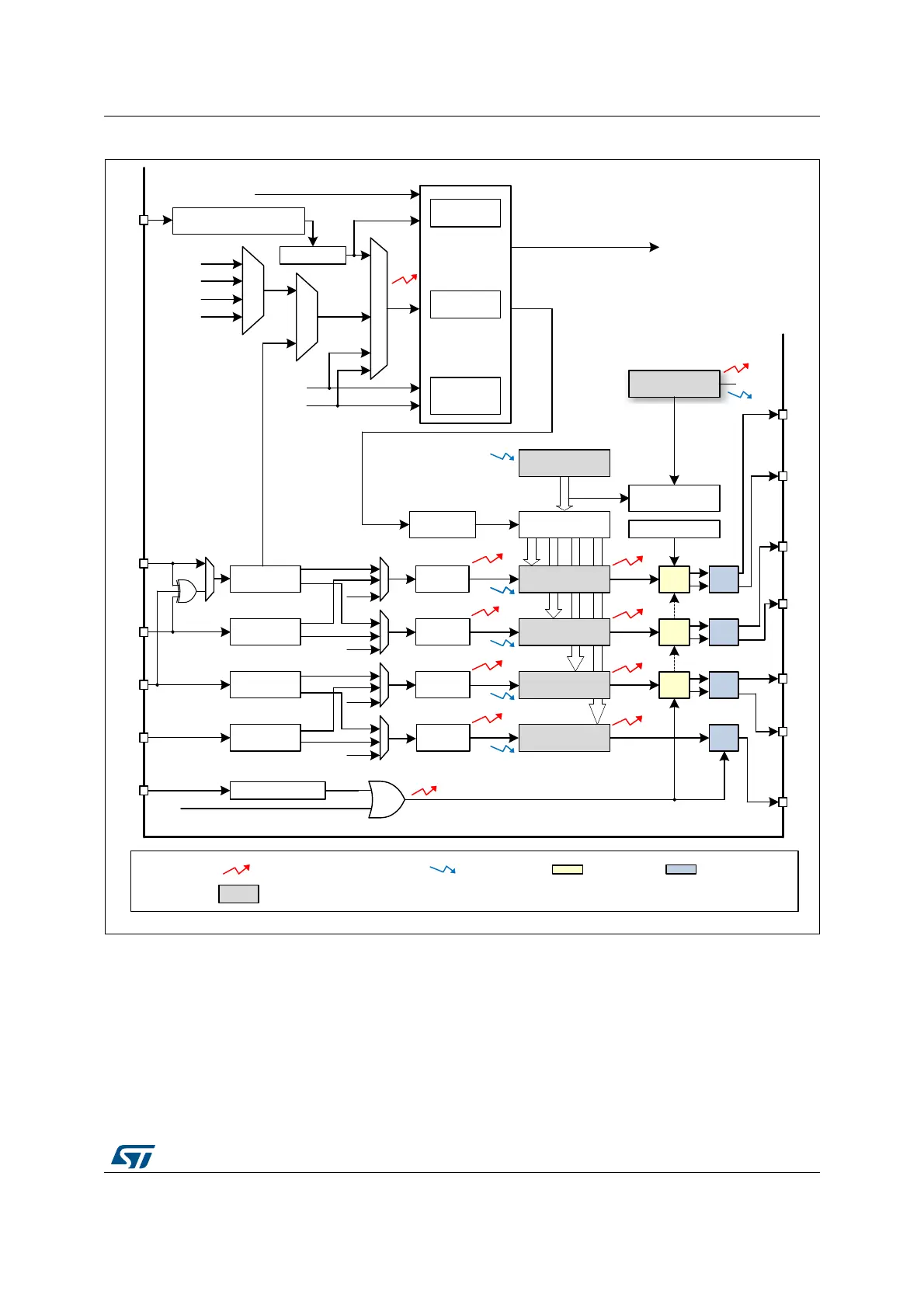
Figure 86. Advanced-control timer block diagram
MS39906V1
Interrupt & DMA output Event
Reg Preload registers transferred to active registers on U event according to control bit
Legend
Polarity selection
Input filter &
Edge detector
Input filter &
Edge detector
Input filter &
Edge detector
Input filter &
Edge detector
TRC
TRC
TRC
TRC
TI4FP4
TI4FP3
TI3FP4
TI3FP3
Prescaler
IC3
IC4
IC2
IC1
Prescaler
Prescaler
Prescaler
TI2FP2
TI2FP1
TI1FP1
TI1FP2
TI1
TI2
TI3
TI4
BRK
Clock failure event from clock controller
CSS (Clock Security System)
IC1PS
IC2PS
IC3PS
IC4PS
BI
Capture/Compare
4 Register
U
Capture/Compare
3 Register
U
U
Capture/Compare
2 Register
Capture/Compare
1 Register
U
CC4I
CC3I
CC2I
CC1I
CC4I
CC3I
CC2I
CC1I
OC1REF
OC2REF
OC3REF
OC4REF
OC4
OC3N
OC3
OC2N
OC2
OC1N
OC1
DTG[7:0] registers
CNT
(counter)
PSC
(prescaler)
CK_CNTCK_PSC
Repetition counter
REP Register
UI
Polarity selection,
Edge detector and Prescaler
Input filter
Trigger
controller
Slave mode
controller
Encoder
interface
Reset,
Enable,
Up/Down,
Count
To other timers
To DAC and ADC
TRGO
TRGI
TGI
Internal clock (CK_INT)
ETRF
ETRP
ETR
CK_TIM18 from RCC
TI1FP1
TI2FP2
TIMx_ETRTIMx_CH1TIMx_CH2TIMx_CH3TIMx_CH4TIMx_BKIN
TIMx_CH1TIMx_CH1NTIMx_CH3TIMx_CH3N TIMx_CH2TIMx_CH4
TIMx_CH2N
U
U
DTG Output control
AutoReload
Register
U
ITR0
ITR1
ITR2
ITR3
TIF_ED