Flexible memory controller (FMC) RM0090
1608/1749 RM0090 Rev 18
The HADDR[25:0] bits contain the external memory address. Since HADDR is a byte
address whereas the memory is addressed at word level, the address actually issued to the
memory varies according to the memory data width, as shown in the following table.
Wrap support for NOR Flash/PSRAM
Wrap burst mode for synchronous memories is not supported. The memories must be
configured in linear burst mode of undefined length.
37.4.2 NAND Flash memory/PC Card address mapping
In this case, three banks are available, each of them being divided into memory areas as
indicated in Table 256.
For NAND Flash memory, the common and attribute memory spaces are subdivided into
three sections (see in Table 257 below) located in the lower 256 Kbytes:
• Data section (first 64 Kbytes in the common/attribute memory space)
• Command section (second 64 Kbytes in the common / attribute memory space)
• Address section (next 128 Kbytes in the common / attribute memory space)
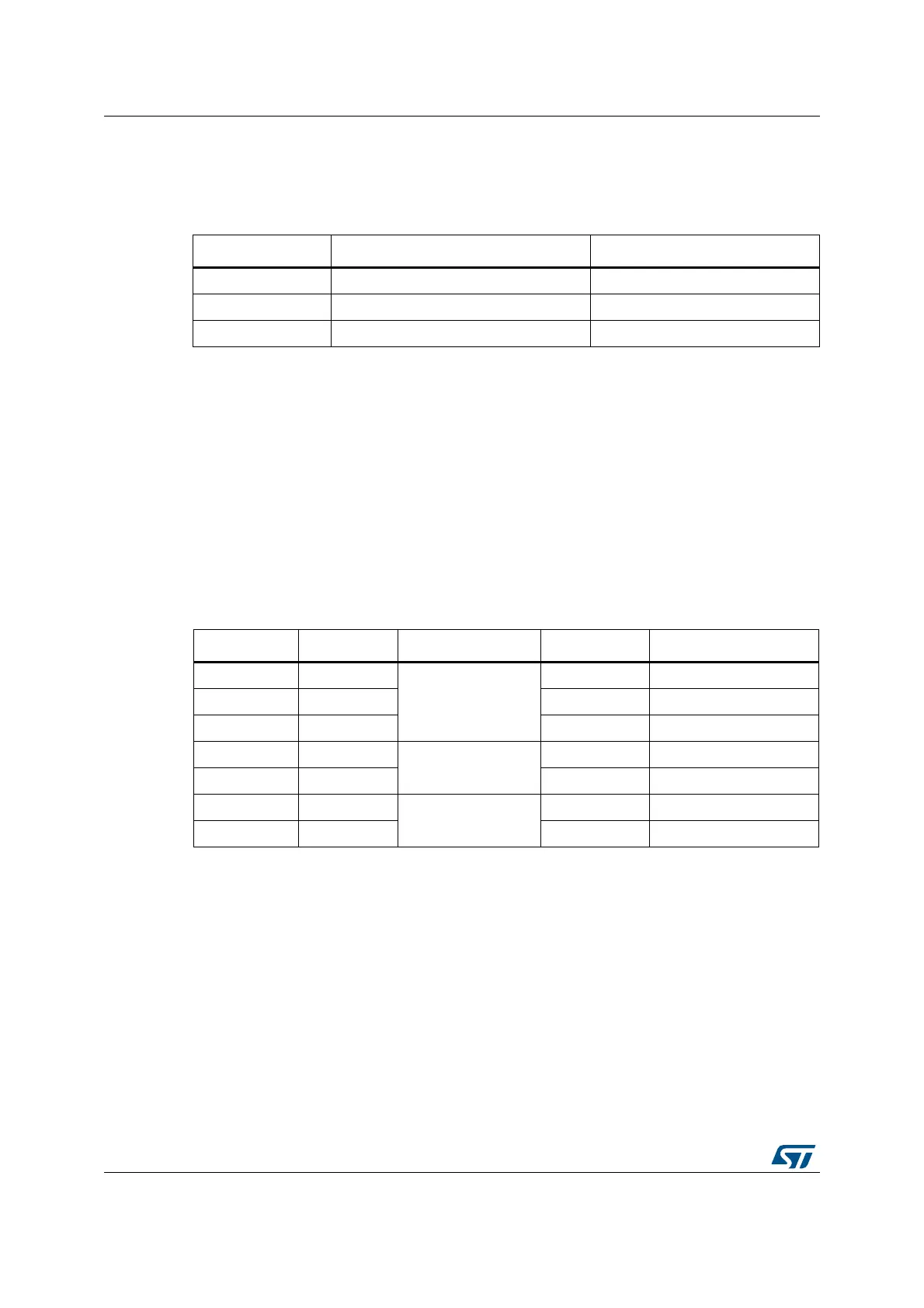
Table 255. NOR/PSRAM External memory address
Memory width
(1)
1. In case of a 16-bit external memory width, the FMC will internally use HADDR[25:1] to generate the
address for external memory FMC_A[24:0].
In case of a 32-bit memory width, the FMC will internally use
HADDR[25:2] to generate the external address.
Whatever the external memory width, FMC_A[0] should be connected to external memory address A[0].
Data address issued to the memory Maximum memory capacity (bits)
8-bit HADDR[25:0] 64 Mbyte x 8 = 512 Mbit
16-bit HADDR[25:1] >> 1 64 Mbyte/2 x 16 = 512 Mbit
32-bit HADDR[25:2] >> 2 64 Mbyte/4 x 32 = 512 Mbit
Table 256. NAND/PC Card memory mapping and timing registers
Start address End address FMC bank Memory space Timing register
0x9C00 0000 0x9FFF FFFF
Bank 4 - PC card
I/O FMC_PIO4 (0xB0)
0x9800 0000 0x9BFF FFFF Attribute FMC_PATT4 (0xAC)
0x9000 0000 0x93FF FFFF Common FMC_PMEM4 (0xA8)
0x8800 0000 0x8BFF FFFF
Bank 3 - NAND Flash
Attribute FMC_PATT3 (0x8C)
0x8000 0000 0x83FF FFFF Common FMC_PMEM3 (0x88)
0x7800 0000 0x7BFF FFFF
Bank 2- NAND Flash
Attribute FMC_PATT2 (0x6C)
0x7000 0000 0x73FF FFFF Common FMC_PMEM2 (0x68)