Digital-to-analog converter (DAC) RM0090
436/1749 RM0090 Rev 18
Figure 65. Data registers in single DAC channel mode
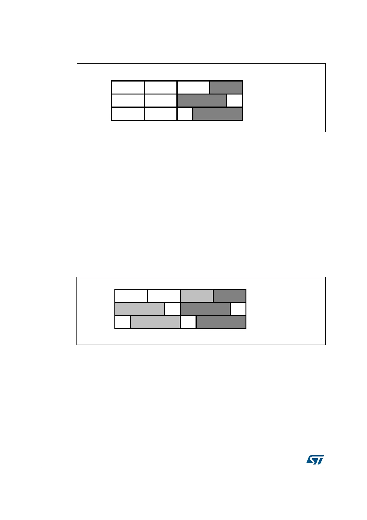
• Dual DAC channels, there are three possibilities:
– 8-bit right alignment: data for DAC channel1 to be loaded into the DAC_DHR8RD
[7:0] bits (stored into the DHR1[11:4] bits) and data for DAC channel2 to be loaded
into the DAC_DHR8RD [15:8] bits (stored into the DHR2[11:4] bits)
– 12-bit left alignment: data for DAC channel1 to be loaded into the DAC_DHR12LD
[15:4] bits (stored into the DHR1[11:0] bits) and data for DAC channel2 to be
loaded into the DAC_DHR12LD [31:20] bits (stored into the DHR2[11:0] bits)
– 12-bit right alignment: data for DAC channel1 to be loaded into the
DAC_DHR12RD [11:0] bits (stored into the DHR1[11:0] bits) and data for DAC
channel2 to be loaded into the DAC_DHR12LD [27:16] bits (stored into the
DHR2[11:0] bits)
Depending on the loaded DAC_DHRyyyD register, the data written by the user is shifted
and stored into DHR1 and DHR2 (data holding registers, which are internal non-memory-
mapped registers). The DHR1 and DHR2 registers are then loaded into the DOR1 and
DOR2 registers, respectively, either automatically, by software trigger or by an external
event trigger.
Figure 66. Data registers in dual DAC channel mode
14.3.4 DAC conversion
The DAC_DORx cannot be written directly and any data transfer to the DAC channelx must
be performed by loading the DAC_DHRx register (write to DAC_DHR8Rx, DAC_DHR12Lx,
DAC_DHR12Rx, DAC_DHR8RD, DAC_DHR12LD or DAC_DHR12LD).
Data stored in the DAC_DHRx register are automatically transferred to the DAC_DORx
register after one APB1 clock cycle, if no hardware trigger is selected (TENx bit in DAC_CR
register is reset). However, when a hardware trigger is selected (TENx bit in DAC_CR
register is set) and a trigger occurs, the transfer is performed three APB1 clock cycles later.
31 24 15 7 0
8-bit right aligned
12-bit left aligned
12-bit right aligned
ai14710b
31 24 15 7 0
8-bit right aligned
12-bit left aligned
12-bit right aligned
ai14709
31 24 15 7 0
8-bit right aligned
12-bit left aligned
12-bit right aligned
ai14709b