Flexible memory controller (FMC) RM0090
1648/1749 RM0090 Rev 18
37.6.1 External memory interface signals
The following tables list the signals that are typically used to interface NAND Flash memory
and PC Card.
Note: The prefix “N” identifies the signals which are active low.
8-bit NAND Flash memory
t
Theoretically, there is no capacity limitation as the FMC can manage as many address
cycles as needed.
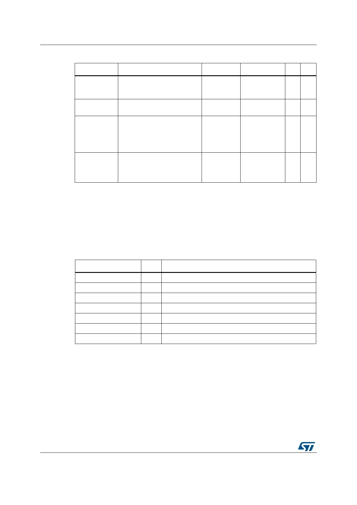
Table 289. Programmable NAND Flash/PC Card access parameters
Parameter Function Access mode Unit Min. Max.
Memory setup
time
Number of clock cycles (HCLK)
required to set up the address
before the command assertion
Read/Write
AHB clock cycle
(HCLK)
1 256
Memory wait
Minimum duration (in HCLK clock
cycles) of the command assertion
Read/Write
AHB clock cycle
(HCLK)
2255
Memory hold
Number of clock cycles (HCLK)
during which the address must be
held (as well as the data if a write
access is performed) after the
command de-assertion
Read/Write
AHB clock cycle
(HCLK)
1 254
Memory
databus high-Z
Number of clock cycles (HCLK)
during which the data bus is kept
in high-Z state after a write
access has started
Write
AHB clock cycle
(HCLK)
1 255
Table 290. 8-bit NAND Flash
FMC signal name I/O Function
A[17] O NAND Flash address latch enable (ALE) signal
A[16] O NAND Flash command latch enable (CLE) signal
D[7:0] I/O 8-bit multiplexed, bidirectional address/data bus
NCE[x] O Chip Select, x = 2, 3
NOE(= NRE) O Output enable (memory signal name: read enable, NRE)
NWE O Write enable
NWAIT/INT[3:2] I NAND Flash ready/busy input signal to the FMC