Flexible static memory controller (FSMC) RM0090
1550/1749 RM0090 Rev 18
For synchronous accesses, the FSMC issues the clock (CLK) to the selected external
device only during the read/write transactions. This clock is a submultiple of the HCLK clock.
The size of each bank is fixed and equal to 64 Mbytes.
Each bank is configured by means of dedicated registers (see Section 36.5.6).
The programmable memory parameters include access timings (see Table 220) and support
for wait management (for PSRAM and NOR Flash accessed in burst mode).
36.5.1 External memory interface signals
Table 221, Table 222 and Table 223 list the signals that are typically used to interface NOR
Flash, SRAM and PSRAM.
Note: Prefix “N”. specifies the associated signal as active low.
NOR Flash, nonmultiplexed I/Os
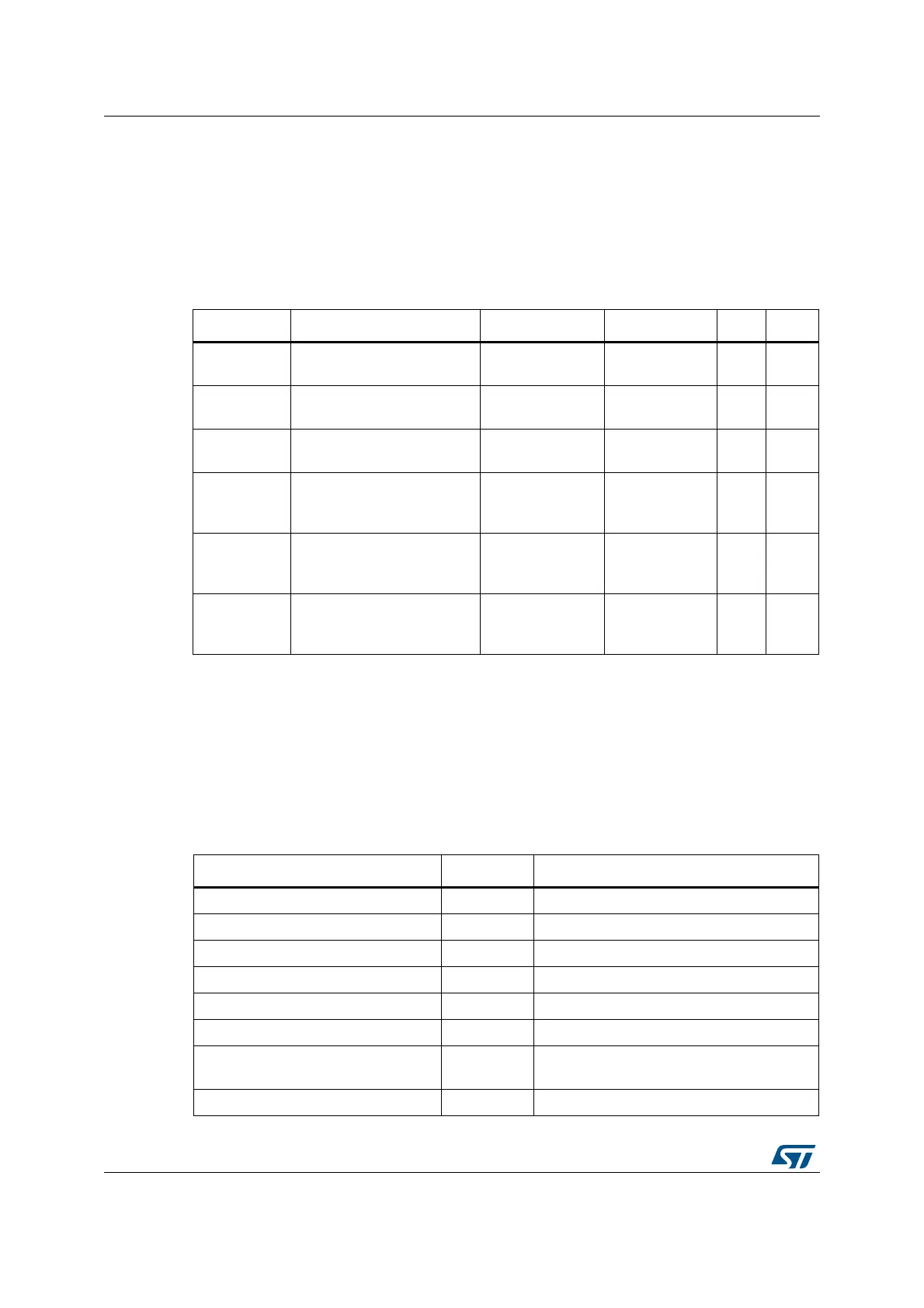
Table 220. Programmable NOR/PSRAM access parameters
Parameter Function Access mode Unit Min. Max.
Address
setup
Duration of the address
setup phase
Asynchronous
AHB clock cycle
(HCLK)
015
Address hold
Duration of the address hold
phase
Asynchronous,
muxed I/Os
AHB clock cycle
(HCLK)
115
Data setup
Duration of the data setup
phase
Asynchronous
AHB clock cycle
(HCLK)
1256
Bus turn
Duration of the bus
turnaround phase
Asynchronous and
synchronous
read/write
AHB clock cycle
(HCLK)
015
Clock divide
ratio
Number of AHB clock cycles
(HCLK) to build one memory
clock cycle (CLK)
Synchronous
AHB clock cycle
(HCLK)
2 16
Data latency
Number of clock cycles to
issue to the memory before
the first data of the burst
Synchronous
Memory clock
cycle (CLK)
2 17
Table 221. Nonmultiplexed I/O NOR Flash
FSMC signal name I/O Function
CLK O Clock (for synchronous access)
A[25:0] O Address bus
D[15:0] I/O Bidirectional data bus
NE[x] O Chip select, x = 1..4
NOE O Output enable
NWE O Write enable
NL(=NADV) O
Latch enable (this signal is called address
valid, NADV, by some NOR Flash devices)
NWAIT I NOR Flash wait input signal to the FSMC