RM0090 Rev 18 899/1749
RM0090 Serial peripheral interface (SPI)
925
28.4 I
2
S functional description
28.4.1 I
2
S general description
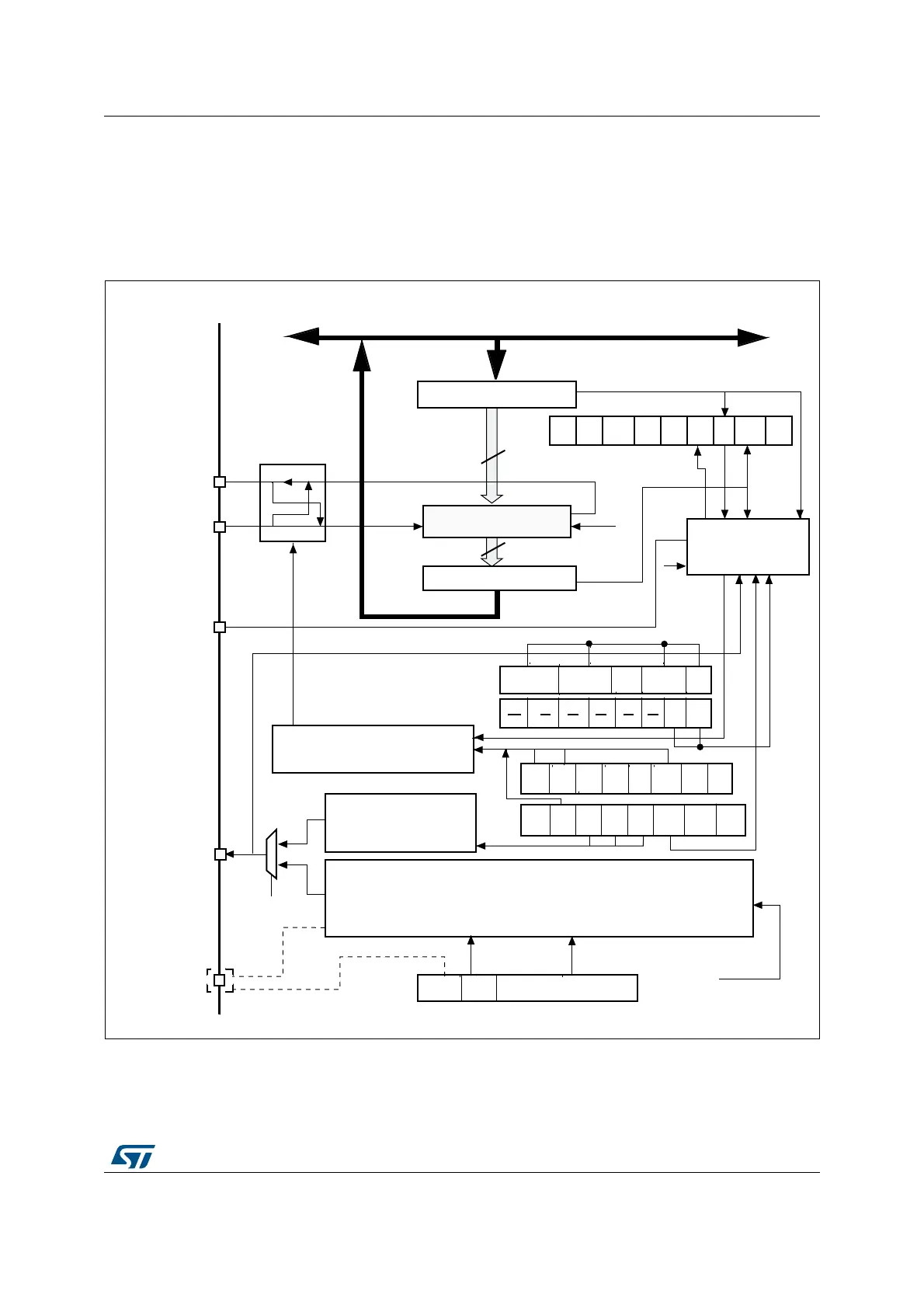
The block diagram of the I
2
S is shown in Figure 262.
Figure 262. I
2
S block diagram
1. I2S2ext_SD and I2S3ext_SD are the extended SD pins that control the I
2
S full duplex mode.
The SPI could function as an audio I
2
S interface when the I
2
S capability is enabled (by
setting the I2SMOD bit in the SPI_I2SCFGR register). This interface uses almost the same
pins, flags and interrupts as the SPI.
Tx buffer
Shift register
16-bit
Communication
Rx buffer
16-bit
MOSI/ SD
Master control logic
MISO/
I2S2ext_SD/
I2S3ext_SD
(1)
SPI
baud rate generator
CK
I2SMOD
LSB first
LSB
First
SPE BR2 BR1 BR0
MSTR CPOL CPHA
Bidi
mode
Bidi
OE
CRC
EN
CRC
Next
DFF
Rx
only
SSM
SSI
Address and data bus
control
NSS/WS
BSY OVR MODF
CRC
ERR
CH
SIDE
TxE RxNE
I
2
S clock generator
MCK
I2S_CK
I2S
MOD
I2SE
CH
DATLEN
LEN
CK
POL
I2SCFG I2SSTD
MCKOEODD I2SDIV[7:0]
[1:0] [1:0]
[1:0]
UDR
I2SxCLK
MS19909V1
FRE