Reset and clock control for STM32F405xx/07xx and STM32F415xx/17xx(RCC) RM0090
262/1749 RM0090 Rev 18
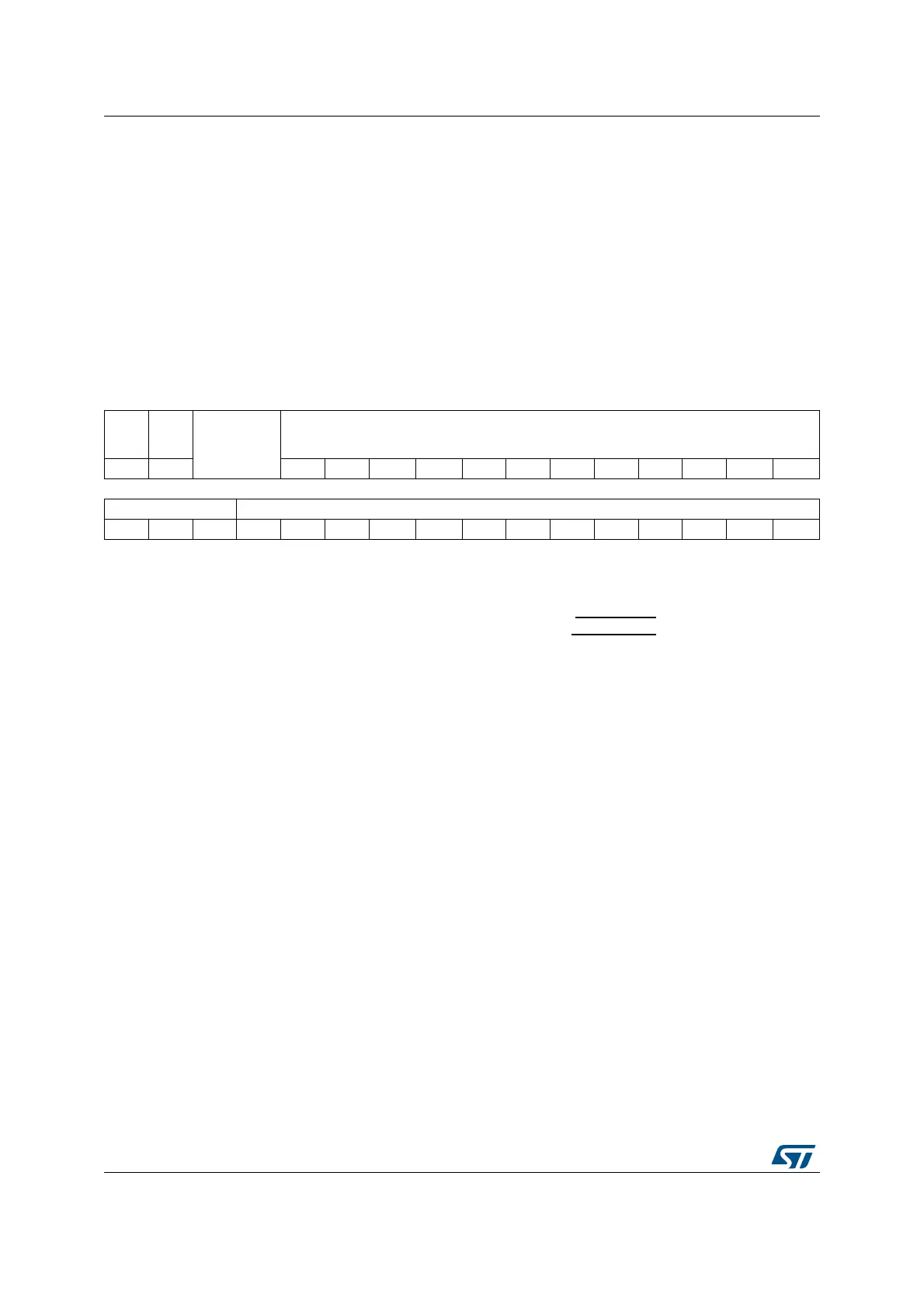
7.3.22 RCC spread spectrum clock generation register (RCC_SSCGR)
Address offset: 0x80
Reset value: 0x0000 0000
Access: no wait state, word, half-word and byte access.
The spread spectrum clock generation is available only for the main PLL.
The RCC_SSCGR register must be written either before the main PLL is enabled or after
the main PLL disabled.
Note: For full details about PLL spread spectrum clock generation (SSCG) characteristics, refer to
the “Electrical characteristics” section in your device datasheet.
31 30 29 28 27 26 25 24 23 22 21 20 19 18 17 16
SSCG
EN
SPR
EAD
SEL
Reserved
INCSTEP
rw rw rw rw rw rw rw rw rw rw rw rw rw
1514131211109 8 7654321 0
INCSTEP MODPER
rw rw rw rw rw rw rw rw rw rw rw rw rw rw rw rw
Bit 31 SSCGEN: Spread spectrum modulation enable
Set and cleared by software.
0: Spread spectrum modulation DISABLE. (To write after clearing CR[24]=PLLON bit)
1: Spread spectrum modulation ENABLE. (To write before setting CR[24]=PLLON bit)
Bit 30 SPREADSEL: Spread Select
Set and cleared by software.
To write before to set CR[24]=PLLON bit.
0: Center spread
1: Down spread
Bits 29:28 Reserved, must be kept at reset value.
Bits 27:13 INCSTEP: Incrementation step
Set and cleared by software. To write before setting CR[24]=PLLON bit.
Configuration input for modulation profile amplitude.
Bits 12:0 MODPER: Modulation period
Set and cleared by software. To write before setting CR[24]=PLLON bit.
Configuration input for modulation profile period.