Digital camera interface (DCMI) RM0090
458/1749 RM0090 Rev 18
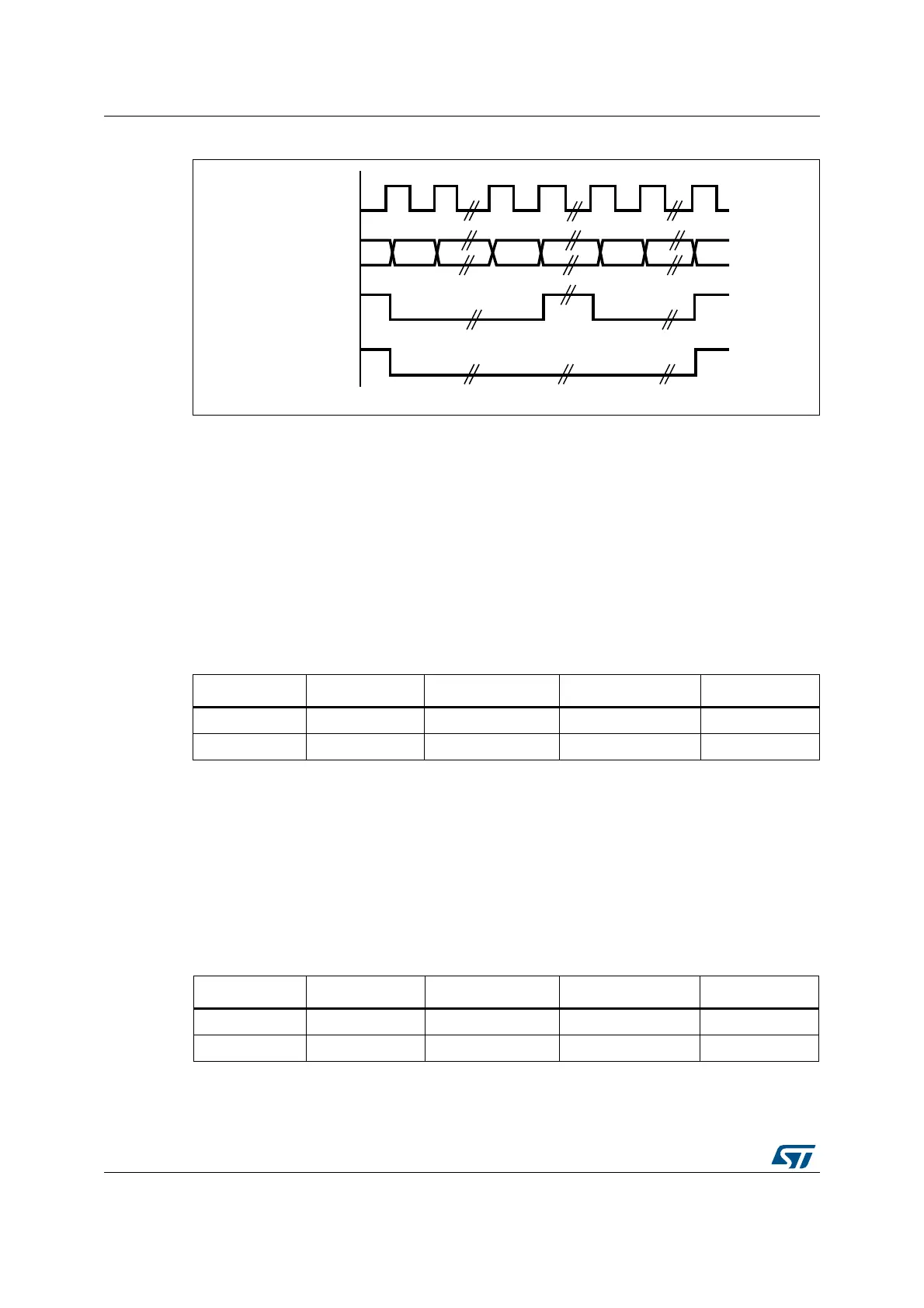
Figure 74. DCMI signal waveforms
1. The capture edge of DCMI_PIXCLK is the falling edge, the active state of DCMI_HSYNC and
DCMI_VSYNC is 1.
1. DCMI_HSYNC and DCMI_VSYNC can change states at the same time.
8-bit data
When EDM[1:0] in DCMI_CR are programmed to “00” the interface captures 8 LSB’s at its
input (D[0:7]) and stores them as 8-bit data. The D[13:8] inputs are ignored. In this case, to
capture a 32-bit word, the camera interface takes four pixel clock cycles.
The first captured data byte is placed in the LSB position in the 32-bit word and the 4
th
captured data byte is placed in the MSB position in the 32-bit word. Table 79 gives an
example of the positioning of captured data bytes in two 32-bit words.
10-bit data
When EDM[1:0] in DCMI_CR are programmed to “01”, the camera interface captures 10-bit
data at its input D[0..9] and stores them as the 10 least significant bits of a 16-bit word. The
remaining most significant bits in the DCMI_DR register (bits 11 to 15) are cleared to zero.
So, in this case, a 32-bit data word is made up every two pixel clock cycles.
The first captured data are placed in the LSB position in the 32-bit word and the 2
nd
captured data are placed in the MSB position in the 32-bit word as shown in Table 80.
Table 79. Positioning of captured data bytes in 32-bit words (8-bit width)
Byte address 31:24 23:16 15:8 7:0
0D
n+3
[7:0] D
n+2
[7:0] D
n+1
[7:0] D
n
[7:0]
4D
n+7
[7:0] D
n+6
[7:0] D
n+5
[7:0] D
n+4
[7:0]
Table 80. Positioning of captured data bytes in 32-bit words (10-bit width)
Byte address 31:26 25:16 15:10 9:0
00D
n+1
[9:0] 0 D
n
[9:0]
40D
n+3
[9:0] 0 D
n+2
[9:0]
DCMI_PIXCLK
DCMI_DR[0:13]
DCMI_HSYNC
DCMI_VSYNC
ai15606b