USB on-the-go full-speed (OTG_FS) RM0090
1266/1749 RM0090 Rev 18
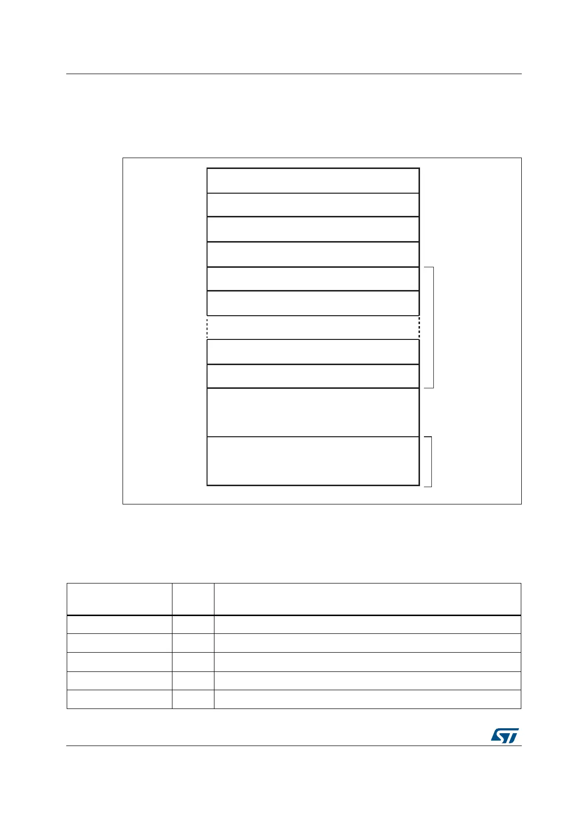
34.16.1 CSR memory map
The host and device mode registers occupy different addresses. All registers are
implemented in the AHB clock domain.
Figure 395. CSR memory map
1. x = 3 in device mode and x = 7 in host mode.
Global CSR map
These registers are available in both host and device modes.
0000h
Core global CSRs (1 Kbyte)
0400h
Host mode CSRs (1 Kbyte)
0800h
Device mode CSRs (1.5 Kbyte)
0E00h
Power and clock gating CSRs (0.5 Kbyte)
1000h
Device EP 0/Host channel 0 FIFO (4 Kbyte)
2000h
Device EP1/Host channel 1 FIFO (4 Kbyte)
3000h
Device EP (x – 1)
(1)
/Host channel (x – 1)
(1)
FIFO (4 Kbyte)
Device EP x
(1)
/Host channel x
(1)
FIFO (4 Kbyte)
Reserved
DFIFO
push/pop
to this region
2 0000h
3 FFFFh
Direct access to data FIFO RAM
for debugging (128 Kbyte)
DFIFO
debug read/
write to this
region
ai15615b
Table 198. Core global control and status registers (CSRs)
Acronym
Address
offset
Register name
OTG_FS_GOTGCTL 0x000 OTG_FS control and status register (OTG_FS_GOTGCTL) on page 1271
OTG_FS_GOTGINT 0x004 OTG_FS interrupt register (OTG_FS_GOTGINT) on page 1272
OTG_FS_GAHBCFG 0x008 OTG_FS AHB configuration register (OTG_FS_GAHBCFG) on page 1274
OTG_FS_GUSBCFG 0x00C OTG_FS USB configuration register (OTG_FS_GUSBCFG) on page 1275
OTG_FS_GRSTCTL 0x010 OTG_FS reset register (OTG_FS_GRSTCTL) on page 1277