RM0090 Rev 18 1585/1749
RM0090 Flexible static memory controller (FSMC)
1601
36.6.1 External memory interface signals
The following tables list the signals that are typically used to interface NAND Flash and PC
Card.
Note: Prefix “N”. specifies the associated signal as active low.
8-bit NAND Flash
t
There is no theoretical capacity limitation as the FSMC can manage as many address
cycles as needed.
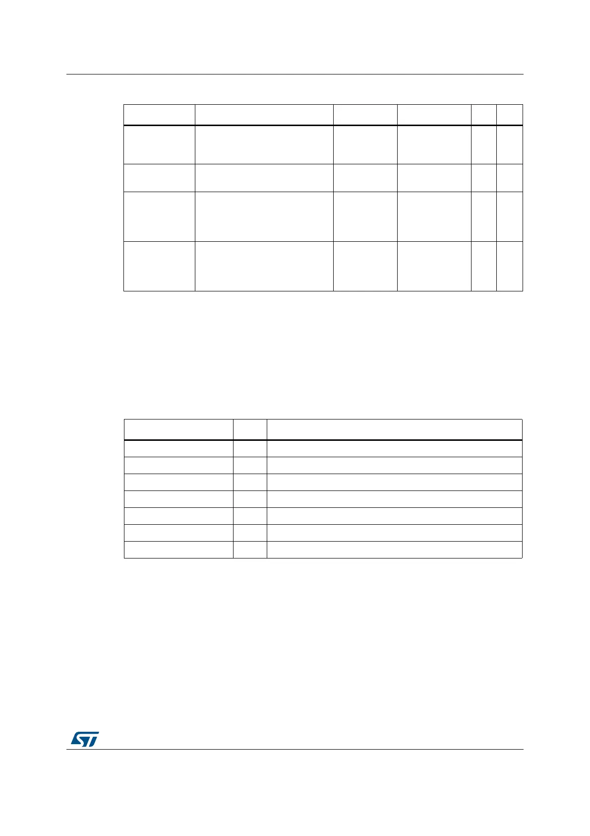
Table 246. Programmable NAND/PC Card access parameters
Parameter Function Access mode Unit Min. Max.
Memory setup
time
Number of clock cycles (HCLK)
to set up the address before the
command assertion
Read/Write
AHB clock cycle
(HCLK)
1 255
Memory wait
Minimum duration (HCLK clock
cycles) of the command assertion
Read/Write
AHB clock cycle
(HCLK)
2 256
Memory hold
Number of clock cycles (HCLK)
to hold the address (and the data
in case of a write access) after
the command de-assertion
Read/Write
AHB clock cycle
(HCLK)
1 254
Memory
databus high-Z
Number of clock cycles (HCLK)
during which the databus is kept
in high-Z state after the start of a
write access
Write
AHB clock cycle
(HCLK)
0 255
Table 247. 8-bit NAND Flash
FSMC signal name I/O Function
A[17] O NAND Flash address latch enable (ALE) signal
A[16] O NAND Flash command latch enable (CLE) signal
D[7:0] I/O 8-bit multiplexed, bidirectional address/data bus
NCE[x] O Chip select, x = 2, 3
NOE(= NRE) O Output enable (memory signal name: read enable, NRE)
NWE O Write enable
NWAIT/INT[3:2] I NAND Flash ready/busy input signal to the FSMC