Basic timers (TIM6 and TIM7) RM0090
702/1749 RM0090 Rev 18
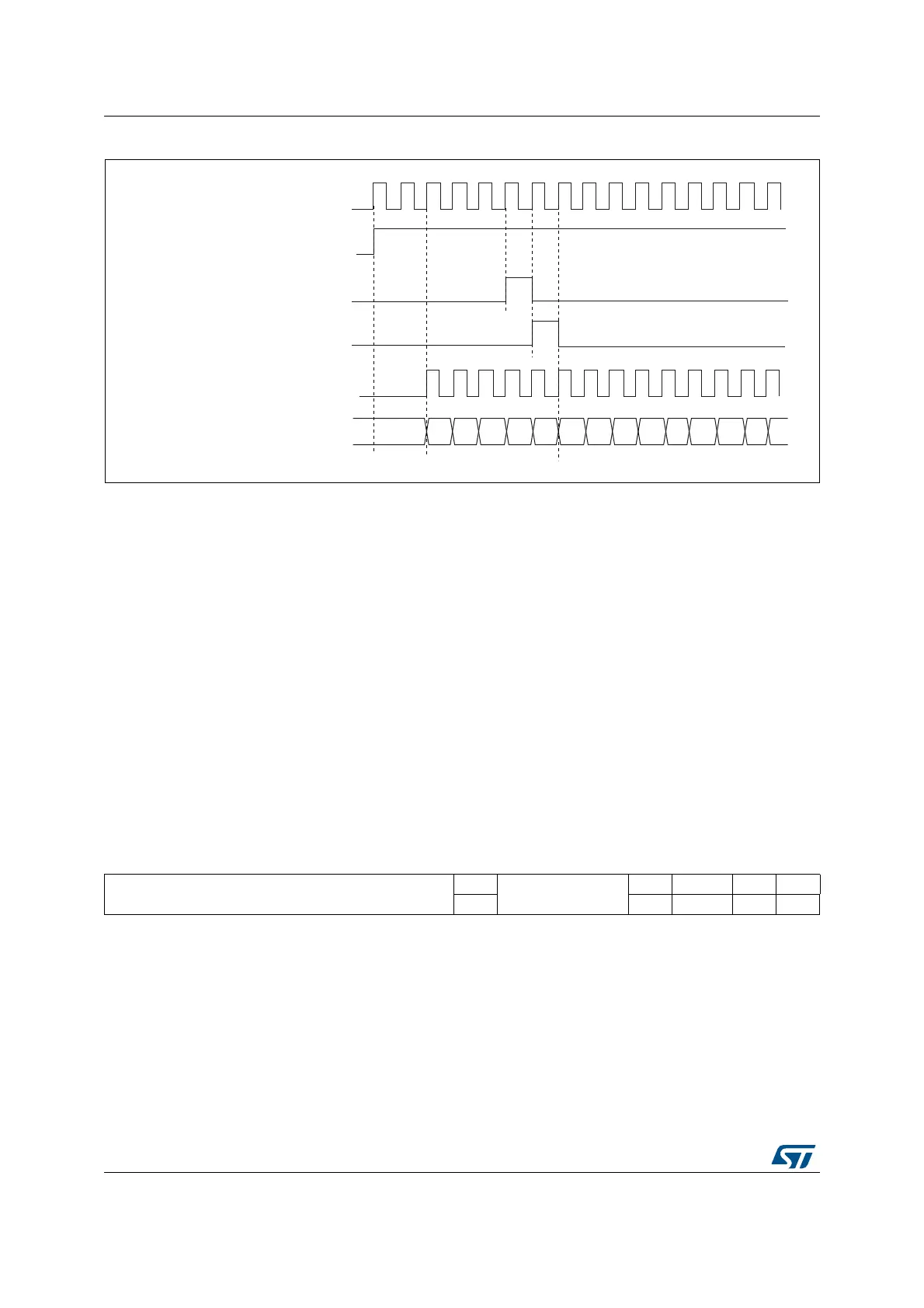
Figure 212. Control circuit in normal mode, internal clock divided by 1
20.3.4 Debug mode
When the microcontroller enters the debug mode (Cortex
®
-M4 with FPU core - halted), the
TIMx counter either continues to work normally or stops, depending on the
DBG_TIMx_STOP configuration bit in the DBG module. For more details, refer to
Section 38.16.2: Debug support for timers, watchdog, bxCAN and I
2
C.
20.4 TIM6 and TIM7 registers
Refer to Section 1.1 for a list of abbreviations used in register descriptions.
The peripheral registers have to be written by half-words (16 bits) or words (32 bits). Read
accesses can be done by bytes (8 bits), half-words (16 bits) or words (32 bits).
20.4.1 TIM6 and TIM7 control register 1 (TIMx_CR1)
Address offset: 0x00
Reset value: 0x0000
Internal clock
Counter clock = CK_CNT = CK_PSC
Counter register
CEN=CNT_EN
UG
CNT_INIT
MS31085V2
00 02
03
04 05
06 0732
33
34 35 36
31
01
15 14 13 12 11 10 9 8 7 6 5 4 3 2 1 0
Reserved
ARPE
Reserved
OPM URS UDIS CEN
rw rw rw rw rw
Bits 15:8 Reserved, must be kept at reset value.
Bit 7 ARPE: Auto-reload preload enable
0: TIMx_ARR register is not buffered.
1: TIMx_ARR register is buffered.
Bits 6:4 Reserved, must be kept at reset value.
Bit 3 OPM: One-pulse mode
0: Counter is not stopped at update event
1: Counter stops counting at the next update event (clearing the CEN bit).