Flexible static memory controller (FSMC) RM0090
1552/1749 RM0090 Rev 18
PSRAM memories are addressed in 16-bit words. The maximum capacity is 512 Mbit (26
address lines).
36.5.2 Supported memories and transactions
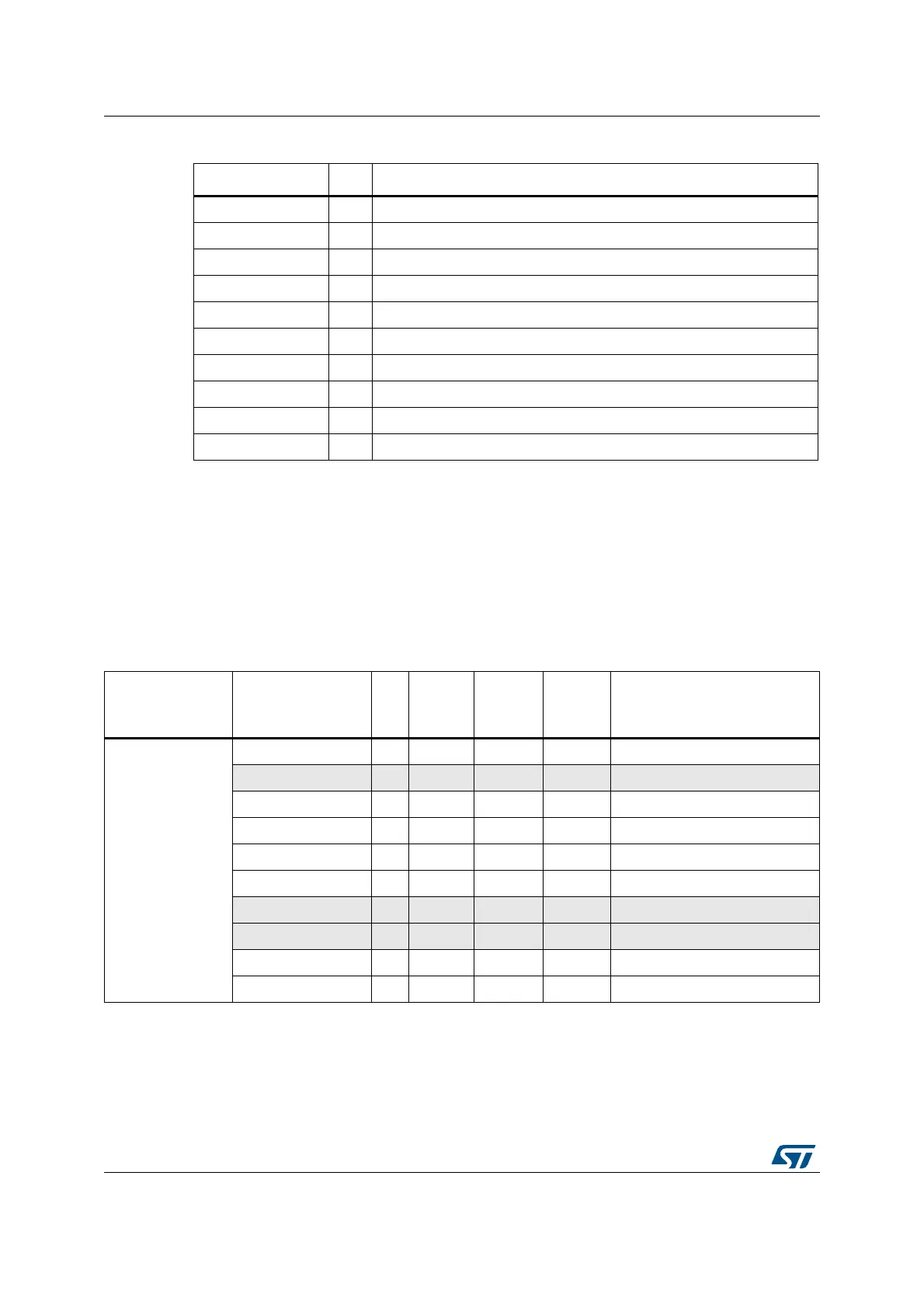
Table 225 below displays an example of the supported devices, access modes and
transactions when the memory data bus is 16-bit for NOR, PSRAM and SRAM.
Transactions not allowed (or not supported) by the FSMC in this example appear in gray.
Table 224. Multiplexed I/O PSRAM
FSMC signal name I/O Function
CLK O Clock (for synchronous access)
A[25:16] O Address bus
AD[15:0] I/O 16-bit multiplexed, bidirectional address/data bus
NE[x] O Chip select, x = 1..4 (called NCE by PSRAM (Cellular RAM i.e. CRAM))
NOE O Output enable
NWE O Write enable
NL(= NADV) O Address valid PSRAM input (memory signal name: NADV)
NWAIT I PSRAM wait input signal to the FSMC
NBL[1] O Upper byte enable (memory signal name: NUB)
NBL[0] O Lowed byte enable (memory signal name: NLB)
Table 225. NOR Flash/PSRAM controller: example of supported memories and transactions
Device Mode R/W
AHB
data
size
Memory
data size
Allowed/
not
allowed
Comments
NOR Flash
(muxed I/Os and
nonmuxed I/Os)
Asynchronous R 8 16 Y -
Asynchronous W 8 16 N -
Asynchronous R 16 16 Y -
Asynchronous W 16 16 Y -
Asynchronous R 32 16 Y Split into two FSMC accesses
Asynchronous W 32 16 Y Split into two FSMC accesses
Asynchronous page R - 16 N Mode is not supported
Synchronous R 8 16 N -
Synchronous R 16 16 Y -
Synchronous R 32 16 Y -