RM0090 Rev 18 1553/1749
RM0090 Flexible static memory controller (FSMC)
1601
36.5.3 General timing rules
Signals synchronization
• All controller output signals change on the rising edge of the internal clock (HCLK)
• In synchronous mode (read or write), all output signals change on the rising edge of
HCLK. Whatever the CLKDIV value, all outputs change as follows:
– NOEL/NWEL/ NEL/NADVL/ NADVH /NBLL/ Address valid outputs change on the
falling edge of FSMC_CLK clock.
– NOEH/ NWEH / NEH/ NOEH/NBLH/ Address invalid outputs change on the rising
edge of FSMC_CLK clock.
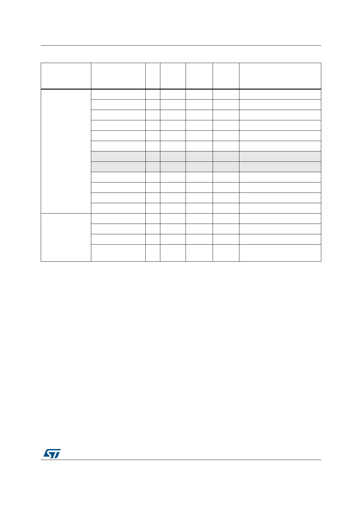
PSRAM
(multiplexed and
nonmultiplexed
I/Os)
Asynchronous R 8 16 Y -
Asynchronous W 8 16 Y Use of byte lanes NBL[1:0]
Asynchronous R 16 16 Y -
Asynchronous W 16 16 Y -
Asynchronous R 32 16 Y Split into two FSMC accesses
Asynchronous W 32 16 Y Split into two FSMC accesses
Asynchronous page R - 16 N Mode is not supported
Synchronous R 8 16 N -
Synchronous R 16 16 Y -
Synchronous R 32 16 Y -
Synchronous W 8 16 Y Use of byte lanes NBL[1:0]
Synchronous W 16 / 32 16 Y -
SRAM and ROM
Asynchronous R 8 / 16 16 Y -
Asynchronous W 8 / 16 16 Y Use of byte lanes NBL[1:0]
Asynchronous R 32 16 Y Split into two FSMC accesses
Asynchronous W 32 16 Y
Split into two FSMC accesses.
Use of byte lanes NBL[1:0]
Table 225. NOR Flash/PSRAM controller: example of supported memories and transactions
Device Mode R/W
AHB
data
size
Memory
data size
Allowed/
not
allowed
Comments