RM0090 Rev 18 1113/1749
RM0090 Controller area network (bxCAN)
1121
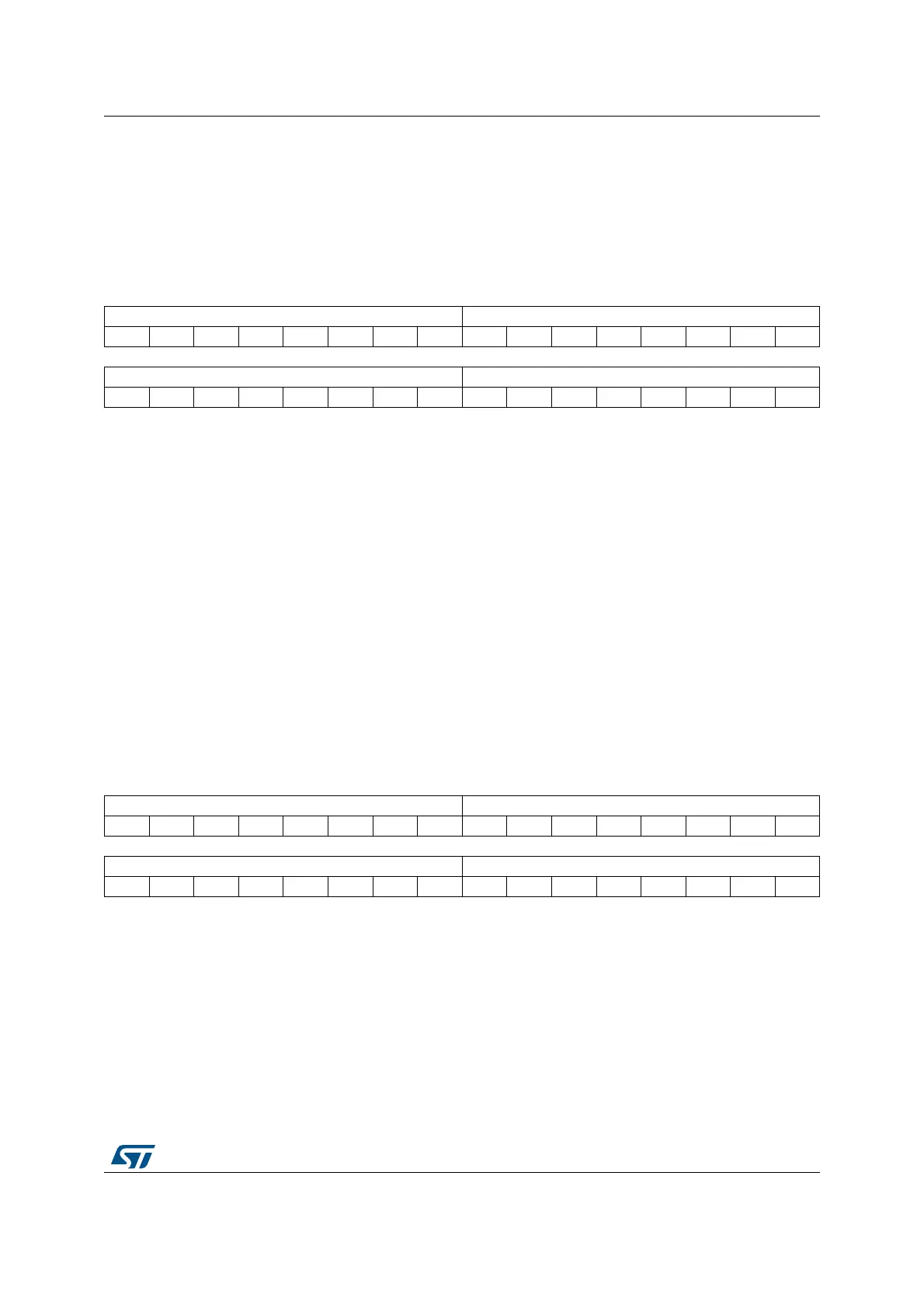
CAN receive FIFO mailbox data low register (CAN_RDLxR) (x=0..1)
All bits of this register are write protected when the mailbox is not in empty state.
Address offsets: 0x1B8, 0x1C8
Reset value: 0xXXXX XXXX
All RX registers are write protected.
CAN receive FIFO mailbox data high register (CAN_RDHxR) (x=0..1)
Address offsets: 0x1BC, 0x1CC
Reset value: 0xXXXX XXXX
All RX registers are write protected.
31 30 29 28 27 26 25 24 23 22 21 20 19 18 17 16
DATA3[7:0] DATA2[7:0]
rrrrrrrrrrrrrrrr
1514131211109876543210
DATA1[7:0] DATA0[7:0]
rrrrrrrrrrrrrrrr
Bits 31:24 DATA3[7:0]: Data Byte 3
Data byte 3 of the message.
Bits 23:16 DATA2[7:0]
: Data Byte 2
Data byte 2 of the message.
Bits 15:8 DATA1[7:0]
: Data Byte 1
Data byte 1 of the message.
Bits 7:0 DATA0[7:0]
: Data Byte 0
Data byte 0 of the message.
A message can contain from 0 to 8 data bytes and starts with byte 0.
31 30 29 28 27 26 25 24 23 22 21 20 19 18 17 16
DATA7[7:0] DATA6[7:0]
rrrrrrrrrrrrrrrr
1514131211109876543210
DATA5[7:0] DATA4[7:0]
rrrrrrrrrrrrrrrr
Bits 31:24 DATA7[7:0]: Data Byte 7
Data byte 3 of the message.
Bits 23:16 DATA6[7:0]
: Data Byte 6
Data byte 2 of the message.
Bits 15:8 DATA5[7:0]
: Data Byte 5
Data byte 1 of the message.
Bits 7:0 DATA4[7:0]
: Data Byte 4
Data byte 0 of the message.