RM0090 Rev 18 357/1749
RM0090 Chrom-Art Accelerator™ controller (DMA2D)
370
11.5.6 DMA2D background memory address register (DMA2D_BGMAR)
Address offset: 0x0014
Reset value: 0x0000 0000
11.5.7 DMA2D background offset register (DMA2D_BGOR)
Address offset: 0x0018
Reset value: 0x0000 0000
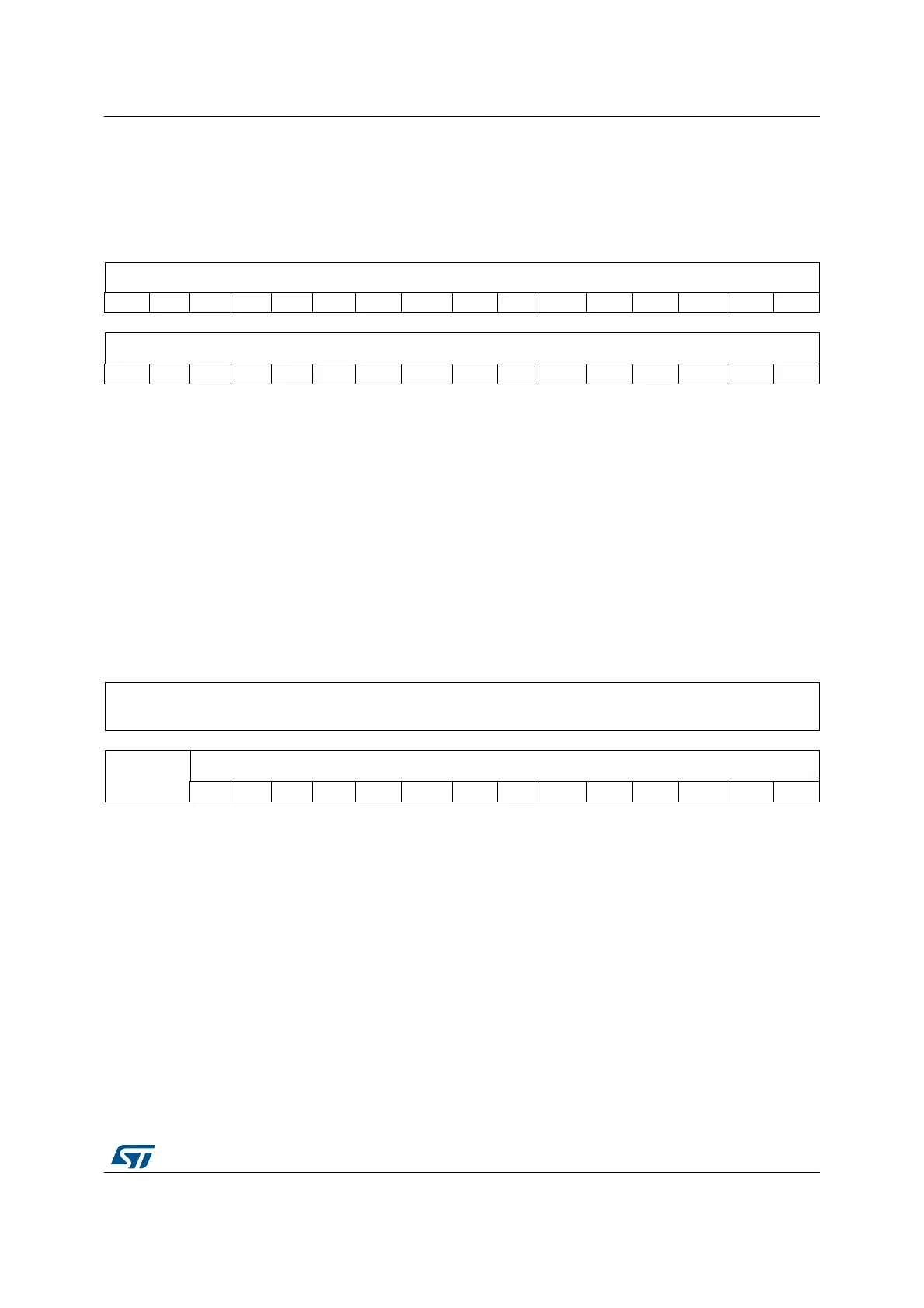
31 30 29 28 27 26 25 24 23 22 21 20 19 18 17 16
MA[31:16]
rw rw rw rw rw rw rw rw rw rw rw rw rw rw rw rw
15 14 13 12 11 10 9 8 7 6 5 4 3 2 1 0
MA[15:0]
rw rw rw rw rw rw rw rw rw rw rw rw rw rw rw rw
Bits 31: 0 MA[31: 0]: Memory address
Address of the data used for the background image. This register can only be written
when data transfers are disabled. Once a data transfer has started, this register is read-
only.
The address alignment must match the image format selected e.g. a 32-bit per pixel
format must be 32-bit aligned, a 16-bit per pixel format must be 16-bit aligned and a 4-
bit per pixel format must be 8-bit aligned.
31 30 29 28 27 26 25 24 23 22 21 20 19 18 17 16
Reserved
15 14 13 12 11 10 9 8 7 6 5 4 3 2 1 0
Reserved
LO[13:0]
rw rw rw rw rw rw rw rw rw rw rw rw rw rw
Bits 31:14 Reserved, must be kept at reset value
Bits 13:0 LO[13: 0]: Line offset
Line offset used for the background image (expressed in pixel). This value is used for
the address generation. It is added at the end of each line to determine the starting
address of the next line.
These bits can only be written when data transfers are disabled. Once data transfer has
started, they become read-only.
If the image format is 4-bit per pixel, the line offset must be even.