Flexible memory controller (FMC) RM0090
1658/1749 RM0090 Rev 18
Common memory space timing register 2..4 (FMC_PMEM2..4)
Address offset: Address: 0x48 + 0x20 * (x – 1), x = 2..4
Reset value: 0xFCFC FCFC
Each FMC_PMEMx (x = 2..4) read/write register contains the timing information for PC Card
or NAND Flash memory bank x. This information is used to access either the common
memory space of the 16-bit PC Card/CompactFlash, or the NAND Flash for command,
address write access and data read/write access.
Bit 4 ILEN: Interrupt high-level detection enable bit
0: Interrupt high-level detection request disabled
1: Interrupt high-level detection request enabled
Bit 3 IREN: Interrupt rising edge detection enable bit
0: Interrupt rising edge detection request disabled
1: Interrupt rising edge detection request enabled
Bit 2 IFS: Interrupt falling edge status
The flag is set by hardware and reset by software.
0: No interrupt falling edge occurred
1: Interrupt falling edge occurred
Note:
This bit is set by programming it to 1 by software.
Bit 1 ILS: Interrupt high-level status
The flag is set by hardware and reset by software.
0: No Interrupt high-level occurred
1: Interrupt high-level occurred
Bit 0 IRS: Interrupt rising edge status
The flag is set by hardware and reset by software.
0: No interrupt rising edge occurred
1: Interrupt rising edge occurred
Note:
This bit is set by programming it to 1 by software.
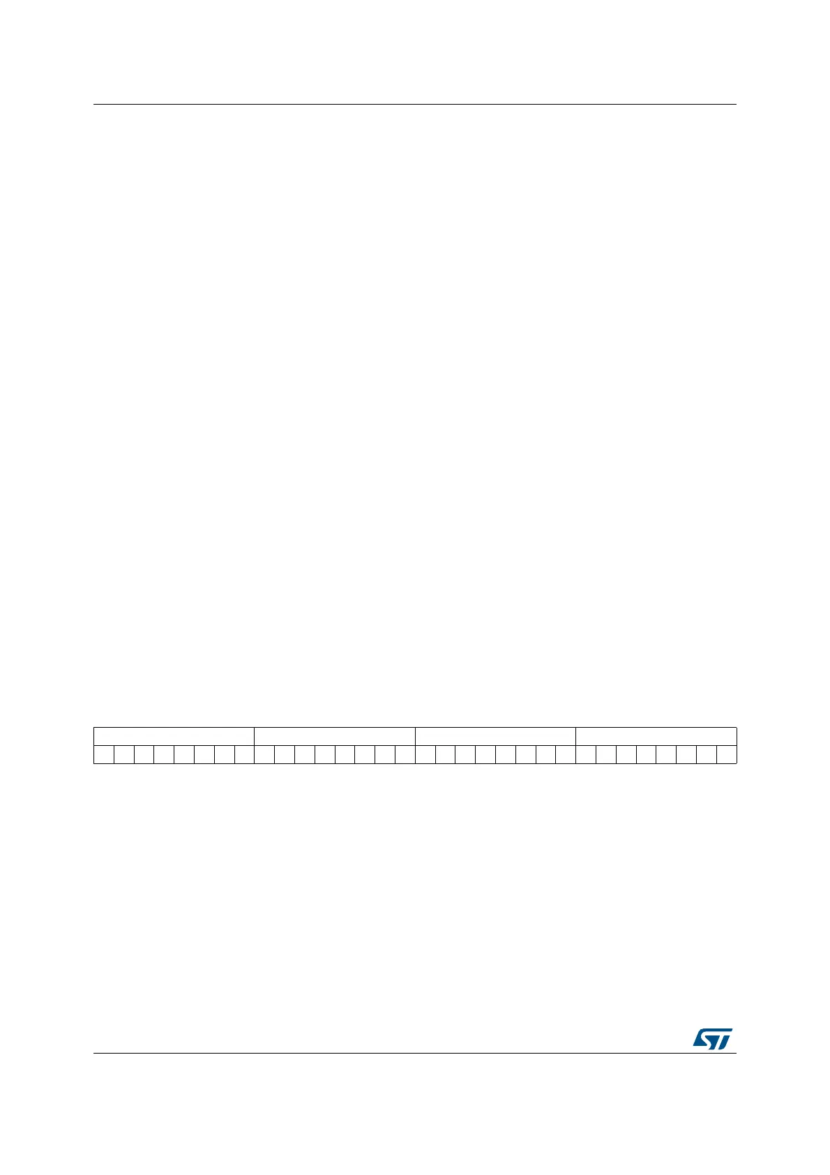
313029282726252423222120191817161514131211109876543210
MEMHIZ[7:0] MEMHOLD[7:0] MEMWAIT[7:0] MEMSET[7:0]
rw rw rw rw rw rw rw rw rw rw rw rw rw rw rw rw rw rw rw rw rw rw rw rw rw rw rw rw rw rw rw rw
Bits 31:24 MEMHIZ[7:0]: Common memory x data bus Hi-Z time
Defines the number of HCLK clock cycles during which the data bus is kept Hi-Z after the
start of a PC Card/NAND Flash write access to common memory space on socket x. This is
only valid for write transactions:
0000 0000: 1 HCLK cycle
1111 1110: 255 HCLK cycles
1111 1111: Reserved.