EZ-USB FX3 Technical Reference Manual, Document Number: 001-76074 Rev. *F 121
General Programmable Interface II (GPIF II)
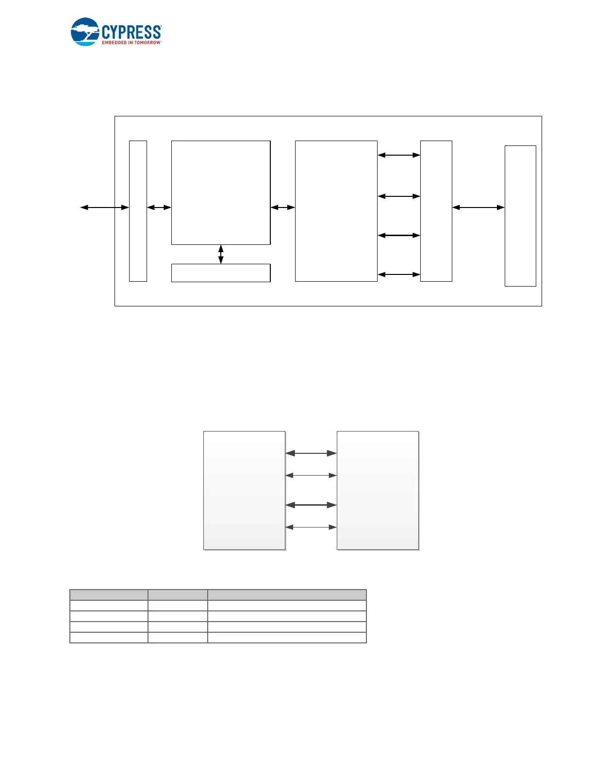
7.2 Block Diagram
Figure 7-1. Block Diagram of FX3 PIB
7.3 Typical GPIF II interface
GPIF II allows the FX3 to connect directly to external peripherals such as FPGAs, image sensors, ADCs, or any other high-
bandwidth devices. It provides external pins that can operate as inputs/outputs (CTL[12:0]), a data bus (DQ[31:0]), an
interface clock (PCLK), and an interrupt line.
Figure 7-2 shows a block diagram of a typical interface between the FX3 and a peripheral function. Ta b l e 7- 1 lists the GPIF II
interface signals.
Figure 7-2. Block Diagram of Interface Between FX3 and Peripheral
Table 7-1. GPIF II Interface Signals
The GPIF II control signals (CTL[12:0]) can be configured as outputs to control the external peripheral device, or as inputs to
read the status from an external peripheral device.
Pin IN/OUT Description
CTL[12:0] I/O Programmable control signals
DQ[31:0] I/O Bidirectional data bus
PCLK I/O Interface clock
INT# /CTL[15] I/O Interrupt or control signal
GPIF-II
DMA Adapter
GPIF-II I/F
THREAD Controller
and Mux Logic
THREAD3
THREAD2
THREAD1
THREAD0
Bus Configuration
Interface
Pins
Read/ Write
access to PIB
sockets
PIB Register Block
PIB Sockets
PIB Block
EZ‐USBFX3
GPIFII
Peripheral
DQ[31:0]
PCLK
CTL[12:0]
INT#/CTL[15]

 Loading...


