EZ-USB FX3 Technical Reference Manual, Document Number: 001-76074 Rev. *F 137
General Programmable Interface II (GPIF II)
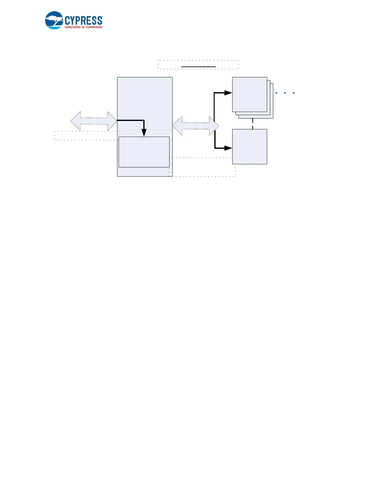
Figure 7-19. GPIF II - PP_MODE=1
7.4.7 Addressing
7.4.7.1 Number of Address Lines
The number of address lines is an important factor in determining the addressing scheme. When the number is eight or more,
the GPIF II Designer tool automatically sets a field, "PP_MODE," which enables an external processor to access some PIB
registers. An example of an interface with eight address lines is the SRAM interface. In this case, the external processor can
directly program the socket and access direction and byte count through the PP_DMA_XFER and PP_DMA_SIZE registers.
When the interface has fewer than eight address lines, access to P-port registers is not possible, and the GPIF II Designer
tool clears the PP_MODE field to 0. For example, this is the case for the Slave FIFO interface, in which, the mapping of
sockets to threads is important, as explained in the following section.
7.4.7.2 Assigning Sockets to Threads
FX3 provides up to four physical threads for data transfer over GPIF II. At a time, any one socket may be mapped to a thread.
For example, in the Slave FIFO implementation, the address signals A0:A1 on the interface indicate the thread to be
accessed. The FX3 DMA fabric will then route the data to the socket mapped to that thread. So if socket 2 is mapped to
thread 2, when A0:A1 = 2, thread 2 is accessed, and any data that is transferred over thread 2 will be routed to socket 2.
Note: In PP_MODE=1, only thread 0 is used. The socket number programmed in the DMA_XFER register gets mapped to
thread 0. In PP_MODE=0, all four threads are accessible. Even though only four physical threads are available, an address
mapping mechanism can be used to access more than four socket addresses. Refer to application note AN68829 - Slave
FIFO Interface for EZ-USB FX3: 5-Bit Address Mode.
7.4.7.3 Addressing Methods
A socket may be addressed directly in PP_MODE =1 by the external processor programming the PP_DMA_XFER register.
Note that when PP_MODE =1, the GPIF II hardware decodes the address based on address bit A7. If A7=1, GPIF II
interprets the access as a register access and performs a read or write to the register address specified by A[7:0]. If A7=0,
then GPIF II interprets the access to be a socket access and performs a read or write operation to the socket number
specified in the PP_DMA_XFER register.
In PP_MODE =0, when the external processor/device does not have access to the PP registers, the thread to be accessed
may be addressed in the following ways. Note that in this case, the corresponding GPIF_THREAD_CONFIG(x) register must
be programmed using the API with the active socket to be accessed.
■ Thread_in_state: Thread address from GPIF II state
GPIFII
up to 32 sockets
accessed through Thread0
T
h
r
e
a
d
0
Socket with
associated
buffers
allocated
If A7=1, GPIFII routes access
to register block
If A7=0, GPIFII routes access
to socket. The socket number
is specified in the
PP_DMA_XFER register
(number of address lines >=8)
A
d
d
r
e
s
s
b
u
s
Address
Comparator
Register Block
PP_MODE = 1

 Loading...


